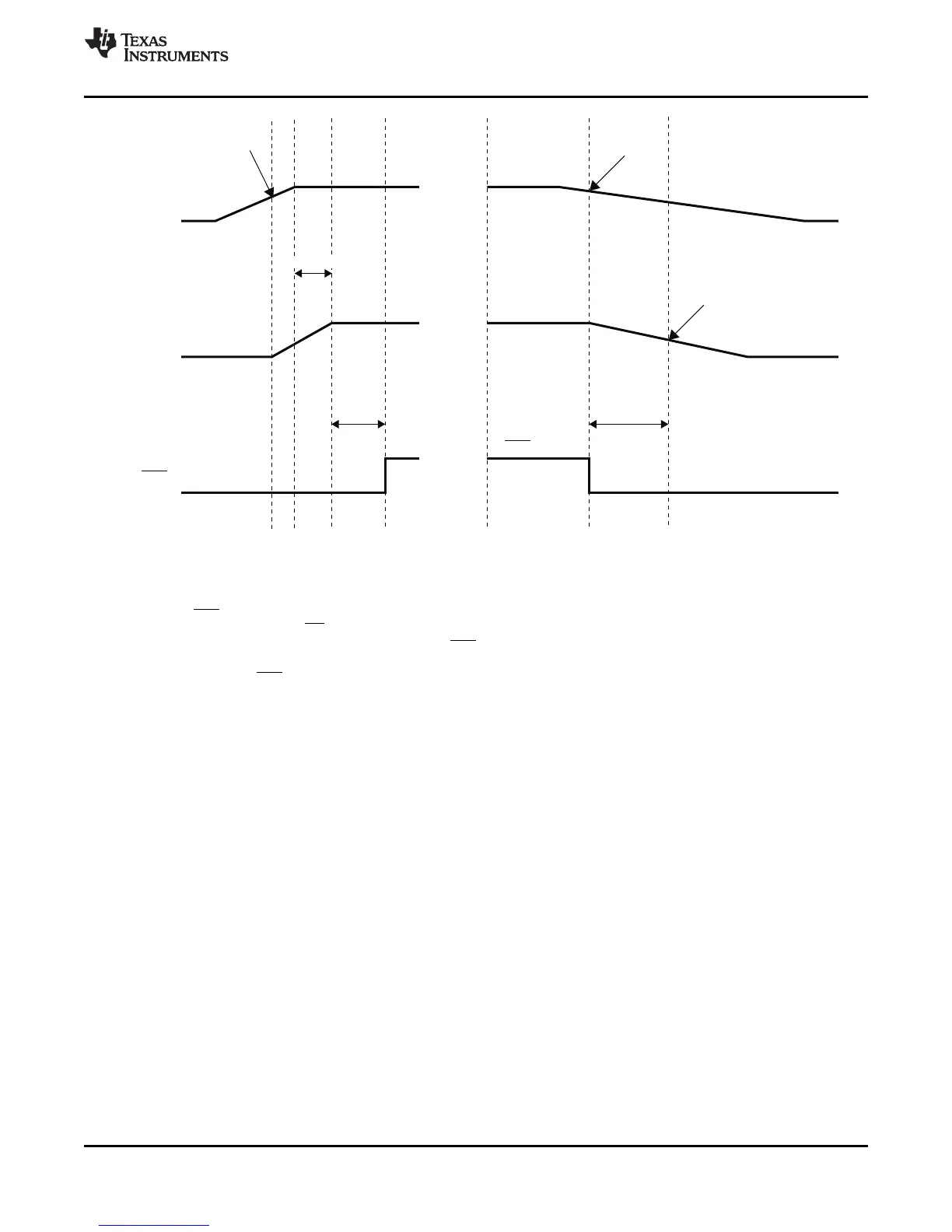
V
DD_3.3V
(A)
2.5 V
(C)
3.3 V
V
DD_1.8V
(B)
XRS
1.8 V
(or 1.9 V)
1.8 V
(or 1.9 V)
XRS
1.5 V
3.3 V
<10 ms
>1 ms
(D)
Power-Up Sequence Power-Down Sequence
(E)
>8 sμ
(F)
TMS320F2810, TMS320F2811, TMS320F2812
TMS320C2810, TMS320C2811, TMS320C2812
www.ti.com
SPRS174T –APRIL 2001–REVISED MAY 2012
A. V
DD_3.3V
– V
DDIO
, V
DD3VFL
, V
DDAIO
, V
DDA1
, V
DDA2
, AVDDREFBG
B. V
DD_1.8V
– V
DD
, V
DD1
C. 1.8-V (or 1.9-V) supply should ramp after the 3.3-V supply reaches at least 2.5 V.
D. Reset (XRS) should remain low until supplies and clocks are stable. See Figure 6-11, Power-on Reset in
Microcomputer Mode (XMP/MC = 0), for minimum requirements.
E. Voltage supervisor or LDO reset control will trip reset (XRS) first when the 3.3-V supply is off regulation. Typically, this
occurs a few milliseconds before the 1.8-V (or 1.9-V) supply reaches 1.5 V.
F. Keeping reset low (XRS) at least 8 µs prior to the 1.8-V (or 1.9-V) supply reaching 1.5 V will keep the flash module in
complete reset before the supplies ramp down.
G. Since the state of GPIO pins is undefined until the 1.8-V (or 1.9-V) supply reaches at least 1 V, this supply should be
ramped as quickly as possible (after the 3.3-V supply reaches at least 2.5 V).
H. Other than the power supply pins, no pin should be driven before the 3.3-V rail has been fully powered up.
Figure 6-6. F2812/F2811/F2810 Typical Power-Up and Power-Down Sequence – Option 2
Copyright © 2001–2012, Texas Instruments Incorporated Electrical Specifications 99
Submit Documentation Feedback
Product Folder Link(s): TMS320F2810 TMS320F2811 TMS320F2812 TMS320C2810 TMS320C2811 TMS320C2812