TMS320F2810, TMS320F2811, TMS320F2812
TMS320C2810, TMS320C2811, TMS320C2812
www.ti.com
SPRS174T –APRIL 2001–REVISED MAY 2012
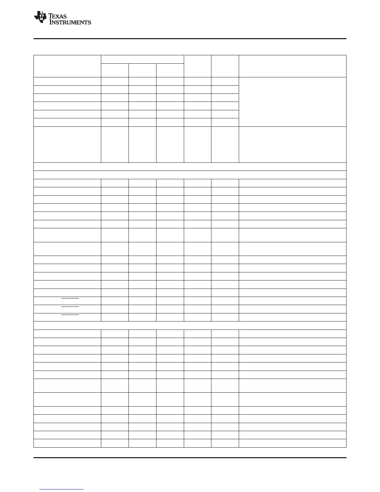
Table 2-2. Signal Descriptions
(1)
(continued)
PIN NO.
NAME I/O/Z
(2)
PU/PD
(3)
DESCRIPTION
179-BALL 176-PIN 128-PIN
GHH/ZHH PGF PBK
V
DDIO
J4 31 25 – –
V
DDIO
L7 64 49 – –
V
DDIO
L10 81 – – –
3 3-V I/O Digital Power Pins
V
DDIO
N14 – – – –
V
DDIO
G11 114 83 – –
V
DDIO
E9 145 104 – –
3.3-V Flash Core Power Pin. This pin should
be connected to 3.3 V at all times after power-
up sequence requirements have been met.
V
DD3VFL
N8 69 52 – –
This pin is used as V
DDIO
in ROM parts and
must be connected to 3.3 V in ROM parts as
well.
GPIO OR PERIPHERAL SIGNALS
GPIOA OR EVA SIGNALS
GPIOA0 - PWM1 (O) M12 92 68 I/O PU GPIO or PWM Output Pin #1
GPIOA1 - PWM2 (O) M14 93 69 I/O PU GPIO or PWM Output Pin #2
GPIOA2 - PWM3 (O) L12 94 70 I/O PU GPIO or PWM Output Pin #3
GPIOA3 - PWM4 (O) L13 95 71 I/O PU GPIO or PWM Output Pin #4
GPIOA4 - PWM5 (O) K11 98 72 I/O PU GPIO or PWM Output Pin #5
GPIOA5 - PWM6 (O) K14 101 75 I/O PU GPIO or PWM Output Pin #6
GPIOA6 -
J11 102 76 I/O PU GPIO or Timer 1 Output
T1PWM_T1CMP (I)
GPIOA7 -
J13 104 77 I/O PU GPIO or Timer 2 Output
T2PWM_T2CMP (I)
GPIOA8 - CAP1_QEP1 (I) H10 106 78 I/O PU GPIO or Capture Input #1
GPIOA9 - CAP2_QEP2 (I) H11 107 79 I/O PU GPIO or Capture Input #2
GPIOA10 - CAP3_QEPI1 (I) H12 109 80 I/O PU GPIO or Capture Input #3
GPIOA11 - TDIRA (I) F14 116 85 I/O PU GPIO or Timer Direction
GPIOA12 - TCLKINA (I) F13 117 86 I/O PU GPIO or Timer Clock Input
GPIOA13 - C1TRIP (I) E13 122 89 I/O PU GPIO or Compare 1 Output Trip
GPIOA14 - C2TRIP (I) E11 123 90 I/O PU GPIO or Compare 2 Output Trip
GPIOA15 - C3TRIP (I) F10 124 91 I/O PU GPIO or Compare 3 Output Trip
GPIOB OR EVB SIGNALS
GPIOB0 - PWM7 (O) N2 45 33 I/O PU GPIO or PWM Output Pin #7
GPIOB1 - PWM8 (O) P2 46 34 I/O PU GPIO or PWM Output Pin #8
GPIOB2 - PWM9 (O) N3 47 35 I/O PU GPIO or PWM Output Pin #9
GPIOB3 - PWM10 (O) P3 48 36 I/O PU GPIO or PWM Output Pin #10
GPIOB4 - PWM11 (O) L4 49 37 I/O PU GPIO or PWM Output Pin #11
GPIOB5 - PWM12 (O) M4 50 38 I/O PU GPIO or PWM Output Pin #12
GPIOB6 -
K5 53 40 I/O PU GPIO or Timer 3 Output
T3PWM_T3CMP (I)
GPIOB7 -
N5 55 41 I/O PU GPIO or Timer 4 Output
T4PWM_T4CMP (I)
GPIOB8 - CAP4_QEP3 (I) M5 57 43 I/O PU GPIO or Capture Input #4
GPIOB9 - CAP5_QEP4 (I) M6 59 44 I/O PU GPIO or Capture Input #5
GPIOB10 - CAP6_QEPI2 (I) P6 60 45 I/O PU GPIO or Capture Input #6
GPIOB11 - TDIRB (I) L8 71 54 I/O PU GPIO or Timer Direction
GPIOB12 - TCLKINB (I) K8 72 55 I/O PU GPIO or Timer Clock Input
Copyright © 2001–2012, Texas Instruments Incorporated Introduction 23
Submit Documentation Feedback
Product Folder Link(s): TMS320F2810 TMS320F2811 TMS320F2812 TMS320C2810 TMS320C2811 TMS320C2812