57
TMS570LS0714
www.ti.com
SPNS226E –JUNE 2013–REVISED NOVEMBER 2016
Submit Documentation Feedback
Product Folder Links: TMS570LS0714
System Information and Electrical SpecificationsCopyright © 2013–2016, Texas Instruments Incorporated
6.6.3 Clock Test Mode
The platform architecture defines a special mode that allows various clock signals to be selected and
output on the ECLK pin and N2HET1[12] device outputs. This special mode, Clock Test Mode, is very
useful for debugging purposes and can be configured through the CLKTEST register in the system
module. See Table 6-14 for the CLKTEST bits value and signal selection.
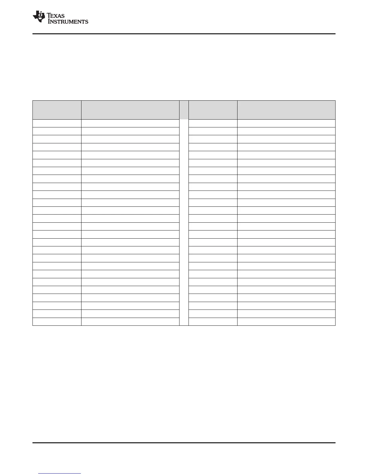
Table 6-14. Clock Test Mode Options
SEL_ECP_PIN
=
CLKTEST[4-0]
SIGNAL ON ECLK
SEL_GIO_PIN
=
CLKTEST[11-8]
SIGNAL ON N2HET1[12]
00000 Oscillator 0000 Oscillator Valid Status
00001 Main PLL free-running clock output 0001 Main PLL Valid status
00010 Reserved 0010 Reserved
00011 EXTCLKIN1 0011 Reserved
00100 LFLPO 0100 Reserved
00101 HFLPO 0101 HFLPO Valid status
00110 Reserved 0110 Reserved
00111 EXTCLKIN2 0111 Reserved
01000 GCLK 1000 LFLPO
01001 RTI Base 1001 Oscillator Valid status
01010 Reserved 1010 Oscillator Valid status
01011 VCLKA1 1011 Oscillator Valid status
01100 VCLKA2 1100 Oscillator Valid status
01101 Reserved 1101 Reserved
01110 Reserved 1110 Reserved
01111 Reserved 1111 Oscillator Valid status
10000 Reserved
10001 HCLK
10010 VCLK
10011 VCLK2
10100 Reserved
10101 VCLK4
10110 Reserved
10111 Reserved
11000 Reserved
Others Reserved