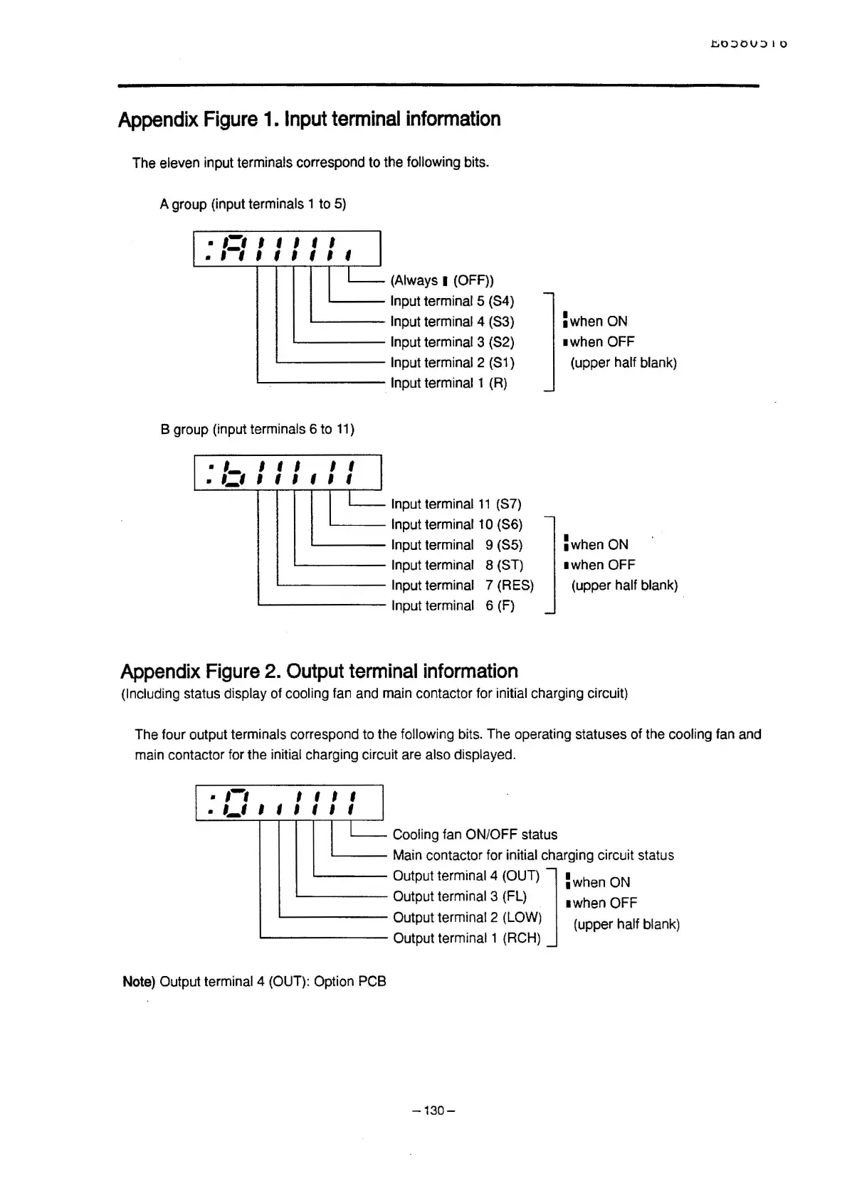
Appendix
Figure
1.
Input
terminal
information
The eleven input terminals correspond to the following bits.
A group (input
terminals 1 to
5)
•
1-1
I I I I I
•
,-,
I I I I I I
(Always I (OFF))
.__
__
Input terminal 5 (S4)
.__
___
Input terminal 4 (S3)
.__
____
Input terminal 3 (S2)
....__
_____
Input terminal 2 (S1)
8 group (input terminals 6 to
11)
.,
,,,
,,
•
l=I
I I I I I I
. Input terminal 1
(R)
Input terminal
11
(S7)
...___
__
Input terminal 1 O (S6)
~---
Input terminal 9
(SS)
.__
____
Input terminal 8 (ST)
....__
_____
Input terminal 7 (RES)
...___
______
Input terminal 6 (F)
Appendix
Figure
2.
Output
terminal
information
:when
ON
1when OFF
(upper half blank)
:when
ON
•when
OFF
(upper half blank)
(Including
status display of cooling fan and main contactor for initial charging circuit)
The four output
terminals correspond
to
the following bits. The operating statuses of the cooling fan and
main contactor for the
initial charging circuit are also displayed.
•
1-1
I I I I
•
1_1
I I I I I I
Cooling fan ON/OFF status
...___
__
Main contactor for initial charging circuit status
Output
terminal 4 (OUT) ] : when
ON
Output terminal 3 (FL) •when OFF
....__
_____
Output terminal 2 (LOW) (upper half blank)
....__
______
Output terminal 1 (RCH)
Note)
Output terminal 4 (OUT): Option PCB
-130-
 Loading...