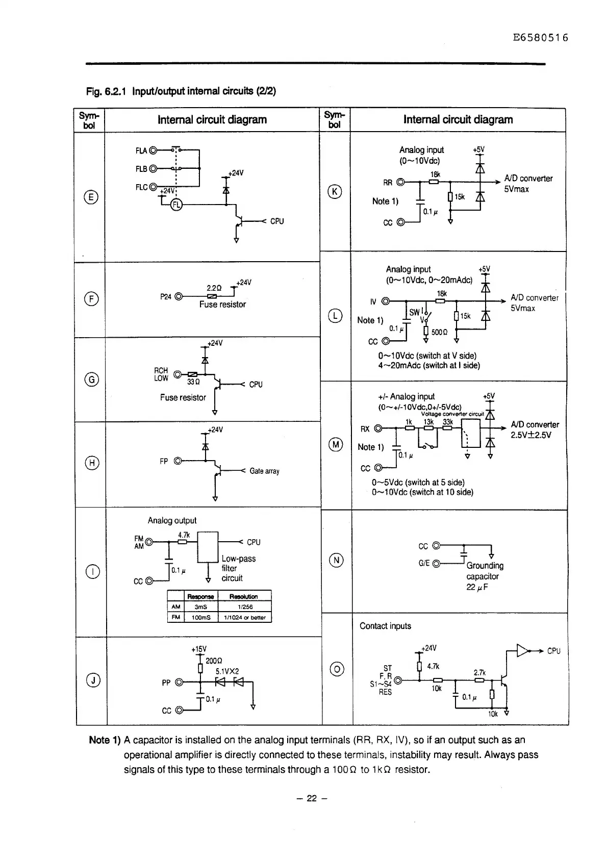
Fig.
6.2.1
Input/output
internal
circuits
(212)
Sym-
bol
®
®
@
®
Internal
circuit
diagram
FLB
o :
RA:t
I
FLC
o +
24
v;
Flt-----+-.
+24V
+24V
_ 2.20 T
P24~
Fuse resistor
RCH
o»--ca-+-,
LOW
330
Fuse resistor
CPU
CPU
Gate
array
Analog output
FM
4.7k
Q))-"""T"-C:>--i
AM
To.1µ
cc~
AM
FM
Response
3mS
100mS
+15V
CPU
Low-pass
filter
circuit
Resolution
11256
111024
cr
better
2000
5.1VX2
To.1µ
cc
@-----J
Sym-
bol
®
@
®
@
E6580516
Internal
circuit
diagram
Analog input
(0-10Vdc)
+5V
18k
RR
o»----c::i----.--+--
AID
converter
5Vmax
15k
Note1)J
0.1
µ
cc
0
Analog input
+5V
(0-1
OVdc,
0-20mAdc)
18k
IV
o»--T--r--O--,r----+--
AID
converter
SWI
5Vmax
Note
1)
V~
15
k
'
0
·
1
µT
sooo
cc
(Q)----1
0-1
OVdc
(switch at V side)
4-20mAdc
(switch at I side)
+I- Analog input
+5V
(0-+/-10Vdc,0+/-5Vdc)
Voltage converter circuit
1k
13k
33k
0.1
µ
Note~1)
cc
0
0-5Vdc
(switch
at
5 side)
0-1
OVdc
(switch at 10 side)
cc© I i
G/E
~Grounding
capacitor
22µF
Contact inputs
+24V
4.7k
ST
s 1
~s'l
o»--+--1=i---..-~2c.7k~--f
RES
10k
0.1
µ
10k
AID
converter
2.5V±2.5V
CPU
Note
1)
A capacitor is installed on the analog input terminals (RR,
RX,
IV), so if
an
output such as
an
operational amplifier is directly connected to these terminals, instability may result. Always pass
signals of this type to these terminals through a 100 O to 1 k O resistor.
-
22
-
 Loading...