op amp U10. The output of U10 modulates the bias
voltage at the bases of 07 and 08. This common emitter
stage provides the voltage gain for the amplifier and
drives the emitter followers, 09 and 01 0. These tran-
sistors provide the current gain and drive capabilities for
the amplifier. The resistor,
R45, and diodes, CR16 and
CR17, serve to keep the output transistors biased on,
thus removing crossover distortion. The output
waveform, which is
20Vp-p maximum, is fed back to the
summing node through the resistors on pins 7 and 6 of
RN2. The capacitors, C50 and C43, and the resistor, R38,
create an active low pass filter with the amplifier. This
helps to improve the signal to noise ratio of the output
waveform. The RC networks of
R48,C51 and R49,C52
improve the frequency response of the amplifier.
4.2.1.1
0
Attenuator
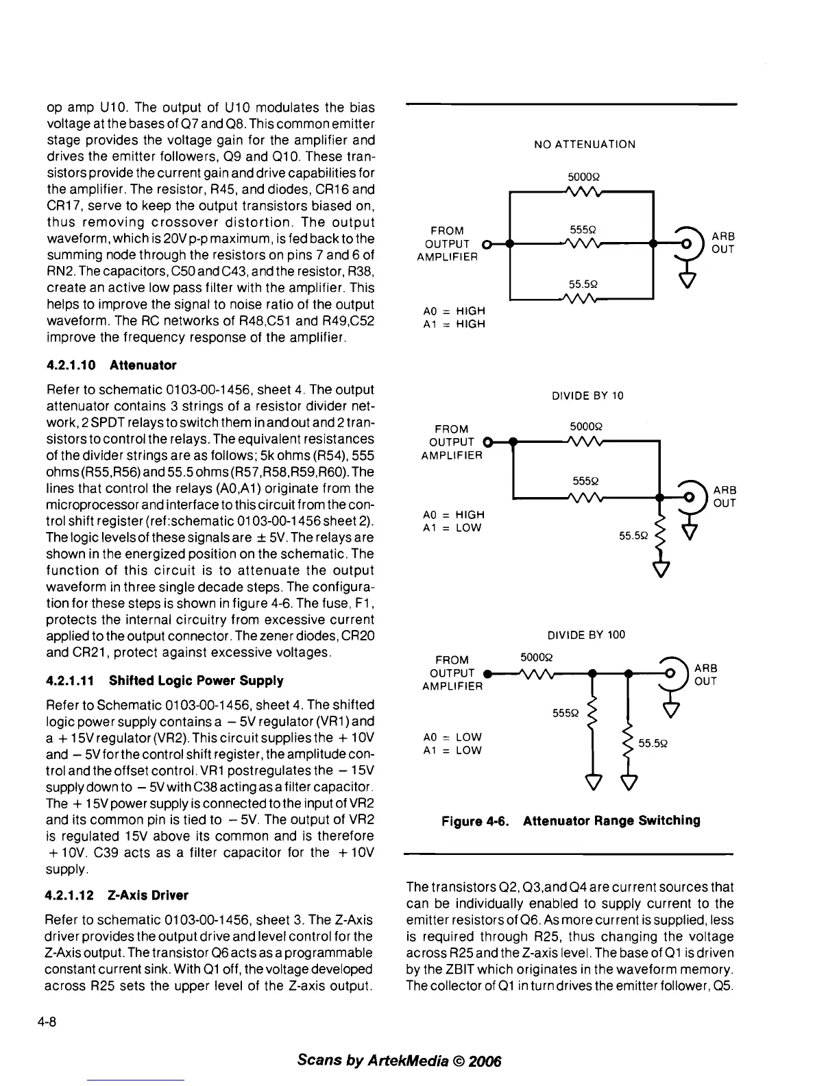
Refer to schematic 0103-00-1456, sheet 4. The output
attenuator contains 3 strings of a resistor divider net-
work,
2SPDT relays toswitch them inandout and 2 tran-
sistors to control the relays. The equivalent resistances
of the divider strings are as follows; 5k ohms
(R54), 555
ohms(R55,R56) and 55.5 ohms(R57,R58,R59,R60). The
lines that control the relays
(A0,Al) originate from the
microprocessor and interface to this circuit from the con-
trol shift register
(ref:schematic 01 03-00-1 456sheet 2).
The logic
levelsof these signals are
+
5V. The relays are
shown in the energized position on the schematic. The
function of this circuit is to attenuate the output
waveform in three single decade steps. The configura-
tion for these steps is shown in figure
4-6. The fuse, F1,
protects the internal circuitry from excessive current
applied to the output connector. Thezener diodes,
CR20
and CR21, protect against excessive voltages.
4.2.1.1 1 Shifted Logic Power Supply
Refer to Schematic 01 03-00-1456, sheet 4. The shifted
logic power supply contains a
-
5V regulator (VRl) and
a
+
15V regulator (VR2). This circuit supplies the
+
1 OV
and
-
5Vforthecontrol shift register, theamplitudecon-
trol and theoffset control. VR1 postregulates the
-
15V
supply down to
-
5VwithC38acting asa filter capacitor.
The
+
15Vpower supply is connected to the input of VR2
and its common pin is tied to
-
5V. The output of VR2
is regulated
15V above its common and is therefore
+
10V. C39 acts as a filter capacitor for the
+
10V
supply.
4.2.1.1 2 Z-Axis Driver
Refer to schematic 01 03-00-1 456, sheet 3. The Z-Axis
driver provides the output drive and level control for the
Z-Axis output. The transistor 06 acts as a programmable
constant current sink. With 01 off, thevoltagedeveloped
across R25 sets the upper level of the Z-axis output.
NO
ATTENUATION
OYZT
ot-*g
;;;
AMPLIFIER
A0
=
HlGH
-
A1
=
HlGH
DIVIDE
BY
10
FROM
500052
OUTPUT
AMPLIFIER
AO=HIGH
A1
=
LOW
'-z3$)"'
DIVIDE BY
100
O
0
Figure 4-6. Attenuator Range Switching
The transistors 02, 03,and 04 are current sources that
can be individually enabled to supply current to the
emitter resistorsof
06. As more current is supplied, less
is required through
R25, thus changing the voltage
across R25 and the Z-axis level. The base of 01 is driven
by the
ZBlT which originates in the waveform memory.
The collector of 01 in turndrives the emitter follower, 05.
Scans
by
Artekhledia
O
2006