7 Series FPGAs GTP Transceivers User Guide www.xilinx.com 33
UG482 (v1.9) December 19, 2016
Reference Clock Selection and Distribution
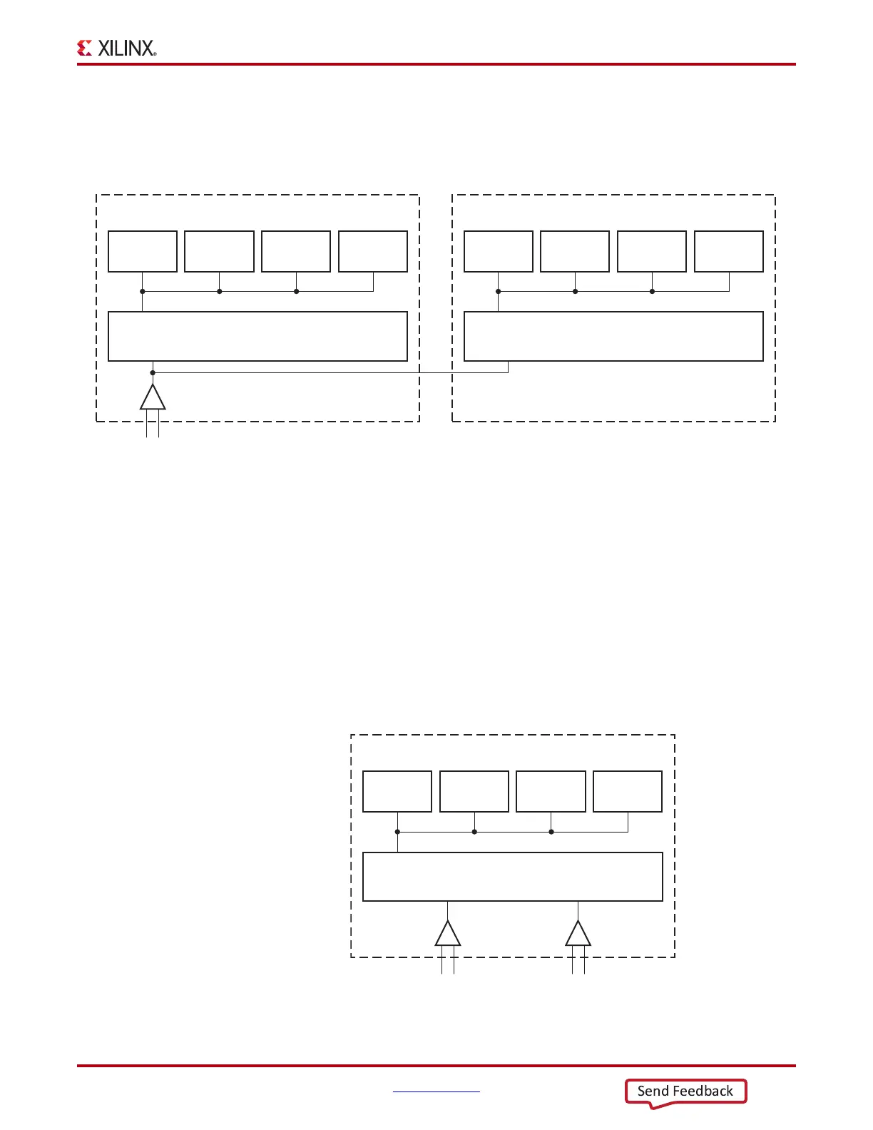
Figure 2-6 shows a single reference clock connected to two GTP Quads. The user connects the
IBUFDS_GTE2 output (O) to the GTREFCLK0 input port of both GTPE2_COMMON primitive
instances. Such a scenario is only possible in the largest Artix-7 device (XC7A200T-FFG1156) that
contains east and west GTP Quads adjacent to each other.
When required, as is the case for the design in Figure 2-6, the Xilinx implementation tools make the
necessary adjustments to the east/west routing shown in Figure 2-2, page 26, as well as any
necessary pin swapping to the GTPE2_COMMON clock inputs to route the reference clocks
between two Quads.
Multiple External Reference Clock Use Model
In Figure 2-7 and Figure 2-9, because the reference clock multiplexer structures in the
GTPE2_COMMON have more than one reference clock source, the user design is required to
connect the output of the IBUFDS_GTE2 to the correct clock input ports on the GTPE2_COMMON
primitive. Figure 2-7 shows an example of a single GTP Quad using both of its dedicated
differential reference clock inputs. Two IBUFDS_GTE2 primitives and a single
GTPE2_COMMON primitive are instantiated.
X-Ref Target - Figure 2-6
Figure 2-6: Two GTP Quads with a Single Shared Reference Clock
UG482_c2_06_110811
GTPE2_
CHANNEL
GTREFCLK0
GTPE2_COMMON
GTPE2_
CHANNEL
GTPE2_
CHANNEL
GTPE2_
CHANNEL
GTP Quad
GTPE2_
CHANNEL
GTREFCLK0
GTPE2_COMMON
GTPE2_
CHANNEL
GTPE2_
CHANNEL
GTPE2_
CHANNEL
GTP Quad
IBUFDS_GTE2
X-Ref Target - Figure 2-7
Figure 2-7: Single GTP Quad using Multiple Local Reference Clocks
UG482_c2_07_110811
GTPE2_
CHANNEL
GTREFCLK0
GTPE2_COMMON
GTPE2_
CHANNEL
GTPE2_
CHANNEL
GTPE2_
CHANNEL
GTP Quad
IBUFDS_GTE2
GTREFCLK1
IBUFDS_GTE2