18 www.xilinx.com Spartan-6 FPGA PCB Design and Pin Planning
UG393 (v1.1) April 29, 2010
Chapter 2: Power Distribution System
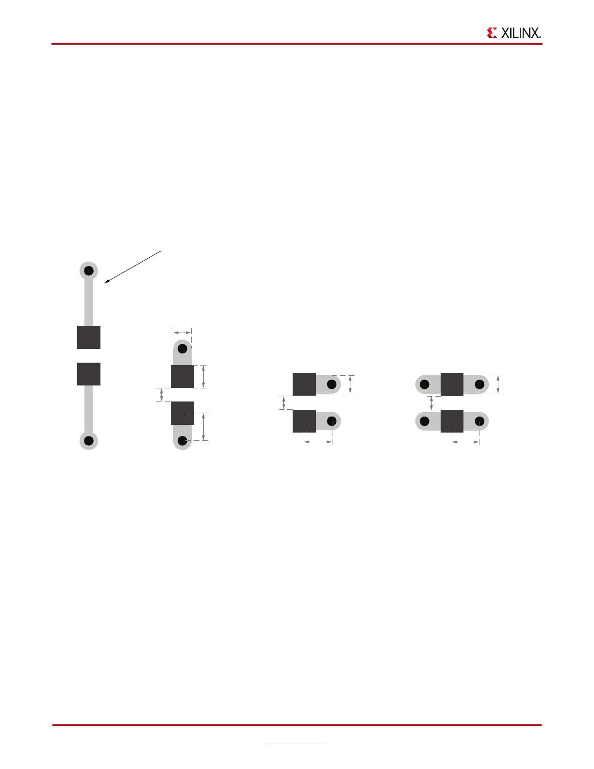
0805 Ceramic Capacitor
The 4.7 µF 0805 capacitor covers the middle frequency range. Placement has some impact
on its performance. The capacitor should be placed as close as possible to the FPGA. Any
placement within two inches of the device’s outer edge is acceptable.
The capacitor mounting (solder lands, traces, and vias) should be optimized for low
inductance. Vias should be butted directly against the pads. Vias can be located at the ends
of the pads (see Figure 2-1B), but are more optimally located at the sides of the pads (see
Figure 2-1C). Via placement at the sides of the pads decreases the mounting’s overall
parasitic inductance by increasing the mutual inductive coupling of one via to the other.
Dual vias can be placed on both sides of the pads (see Figure 2-1D) for even lower parasitic
inductance, but with diminishing returns.
X-Ref Target - Figure 2-1
Figure 2-1: Example 0805 Capacitor Land and Mounting Geometries
0805 Land Pattern
End Vias
Long Traces
(A)
UG393_c2_01_091809
(B)
0805 Land Pattern
End Vias
Not Recommended.
Connecting Trace is Too Long
1.27 mm
(50 mils)
0.61mm
(24 mils)
1.07 mm
(42 mils)
0.61mm
(24 mils)
(C)
0805 Land Pattern
Side Vias
1.12 mm
(44 mils)
0.61 mm
(24 mils)
0.61mm
(24 mils)
(D)
0805 Land Pattern
Double Side Vias
0.61mm
(24 mils)
0.61 mm
(24 mils)
1.12 mm
(44 mils)

 Loading...


