20 www.xilinx.com Spartan-6 FPGA PCB Design and Pin Planning
UG393 (v1.1) April 29, 2010
Chapter 2: Power Distribution System
Basic PDS Principles
The purpose of the PDS and the properties of its components are discussed in this section.
The important aspects of capacitor placement, capacitor mounting, PCB geometry, and
PCB stackup recommendations are also described.
Noise Limits
In the same way that devices in a system have a requirement for the amount of current
consumed by the power system, there is also a requirement for the cleanliness of the
power. This cleanliness requirement specifies a maximum amount of noise present on the
power supply, often referred to as ripple voltage (V
RIPPLE
). Most digital devices, including
all Spartan-6 FPGAs, require that V
CC
supplies not fluctuate more than ±5% of the nominal
V
CC
value. This means that the peak-to-peak V
RIPPLE
must be no more than 10% of the
nominal V
CC
. In this document the term V
CC
is used generically for the following FPGA
power supplies: V
CCINT
, V
CCO
, V
CCAUX
, and V
REF
. This assumes that nominal V
CC
is
exactly the nominal value provided in the data sheet. If not, then V
RIPPLE
must be adjusted
to a value correspondingly less than 10%.
The power consumed by a digital device varies over time and this variance occurs on all
frequency scales, creating a need for a wide-band PDS to maintain voltage stability.
• Low-frequency variance of power consumption is usually the result of devices or
large portions of devices being enabled or disabled. This variance occurs in time
frames from milliseconds to days.
• High-frequency variance of power consumption is the result of individual switching
events inside a device. This occurs on the scale of the clock frequency and the first few
harmonics of the clock frequency up to about 1 GHz.
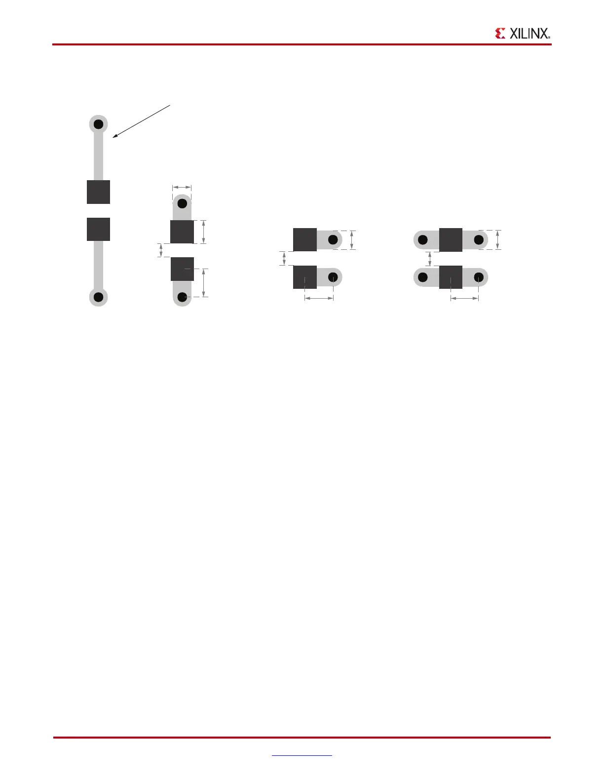
X-Ref Target - Figure 2-2
Figure 2-2: Example 0402 Capacitor Land and Mounting Geometries
0402 Land Pattern
End Vias
Long Traces
(A) (C)(B) (D)
UG393_c2_02_091809
0402 Land Pattern
End Vias
0.381 mm
(15 mils)
0.635 mm
(25 mils)
1.07 mm
(42 mils)
0.61mm
(24 mils)
0402 Land Pattern
Double Side Vias
0.762 mm
(30 mils)
0.381 mm
(15 mils)
0.61mm
(24 mils)
0402 Land Pattern
Side Vias
0.762 mm
(30 mils)
0.381 mm
(15 mils)
0.61mm
(24 mils)
Not Recommended.
Connecting Trace is Too Long

 Loading...


