EasyManuals Logo

Xilinx Spartan-6 FPGA Series User Manual

Xilinx Spartan-6 FPGA Series
72 pages
To Next Page IconTo Next Page
To Previous Page IconTo Previous Page
Page #69 background imageLoading...
Page #69 background image
Spartan-6 FPGA PCB Design and Pin Planning www.xilinx.com 69
UG393 (v1.1) April 29, 2010
Appendix A
Recommended PCB Design Rules
This appendix outlines the recommended design rules for all the available Spartan-6 FPGA
packages.
Recommended PCB Design Rules for QFP Packages
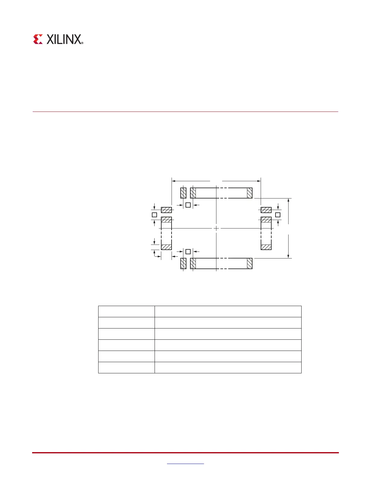
X-Ref Target - Figure A-1
Figure A-1: EIA Standard Board Layout of Soldered Pads for QFP Packages
Tabl e A - 1: PCB Land Pad Dimensions for Quad Flat Pack Packages
(1)
Dimension TQG144
M
ID
19.80
M
IE
19.80
e0.50
b
2
0.3–0.4
I
2
1.60
Notes:
1. Dimensions in millimeters.
ug393_aA_01_030210
M
M
ID
b
2
I
2
M
IE
e
e
e
e

Table of Contents

Questions and Answers:

Question and Answer IconNeed help?

Do you have a question about the Xilinx Spartan-6 FPGA Series and is the answer not in the manual?

Xilinx Spartan-6 FPGA Series Specifications

General IconGeneral
Device FamilySpartan-6
CategoryFPGA
Number of Logic Cells3, 840 to 147, 443
Block RAM216 Kb to 4, 824 Kb
Maximum User I/O102 to 576
Process Technology45nm
Operating Voltage1.2V
Number of DSP Slices8 to 180
Package OptionsFG256, FG484, FG676, FG900, FG1156, FT256, FTG256, FTG484, FTG676, FTG900, FTG1156

Related product manuals