70 www.xilinx.com Spartan-6 FPGA PCB Design and Pin Planning
UG393 (v1.1) April 29, 2010
Appendix A: Recommended PCB Design Rules
Recommended PCB Design Rules for BGA and CSP Packages
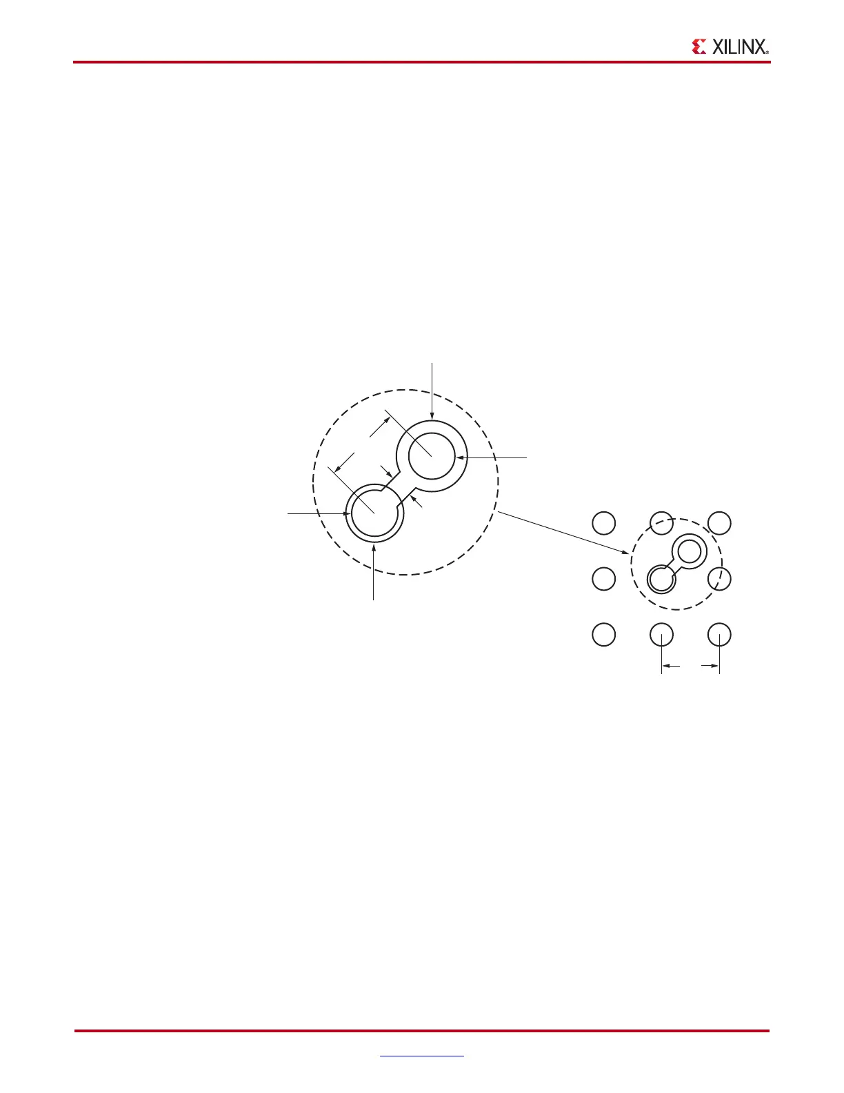
Xilinx provides the diameter of a land pad on the component side. This information is
required prior to the start of the board layout so the board pads can be designed to match
the component-side land geometry. The typical values of these land pads are described in
Figure A-2 and summarized in Table A-2.
For Spartan-6 FPGA BGA packages, non-solder mask defined (NSMD) pads on the board
are suggested to allow a clearance between the land metal (diameter L) and the solder
mask opening (diameter M) as shown in Figure A-2. The space between the NSMD pad
and the solder mask and the actual signal trace widths depends on the capability of the
PCB vendor. The cost of the PCB is higher when the line width and spaces are smaller. In
Figure A-2, the 3 x 3 matrix is for illustration only, one land pad shown with via
connection.
X-Ref Target - Figure A-2
Figure A-2: Suggested Board Layout of Soldered Pads for BGA and CSP Packages
Non Solder Mask Defined Land Patterns or
Land Defined Land Patterns are recommended for FG packages
e
VH
L
M
VL
D
W
Mask Opening
Outside of Land
ug393_aA_01_030210

 Loading...


