Spartan-6 FPGA PCB Design and Pin Planning www.xilinx.com 71
UG393 (v1.1) April 29, 2010
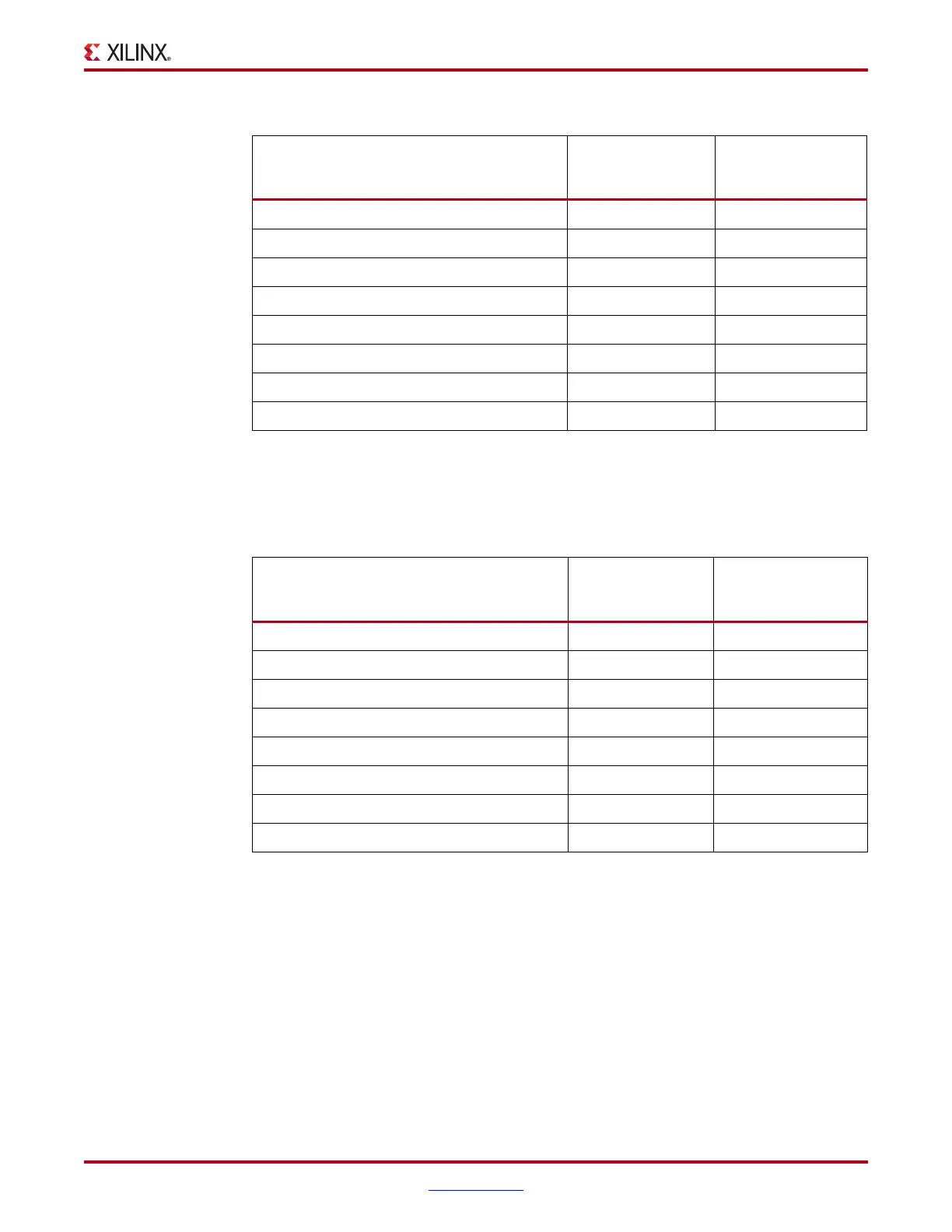
Recommended PCB Design Rules for BGA and CSP Packages
Tabl e A - 2: Recommended PCB Design Rules (mm) for BGA Packages
Design Rule FT(G)256
FG(G)484
FG(G)676
FG(G)900
Component land pad diameter (SMD)
(1)
0.40 0.45
Solder land (L) diameter 0.40 0.40
Opening in solder mask (M) diameter 0.50 0.50
Solder (ball) land pitch (e) 1.00 1.00
Line width between via and land (w) 0.13 0.13
Distance between via and land (D) 0.70 0.70
Via land (VL) diameter 0.61 0.61
Through hole (VH) diameter 0.300 0.300
Notes:
1. Component land pad diameter refers to the pad opening on the component side (solder mask defined).
The space between the NSMD pad and the solder mask, as well as the actual signal trace widths,
depend on the capability of the PCB vendor. PCB costs increase as the line width and spaces become
smaller.
Tabl e A - 3: Recommended PCB Design Rules (mm) for CSP Packages
Design Rule
CSG225
CSG324
CSG484
CPG196
Component land pad diameter (SMD)
(1)
0.40 0.30
Solder land (L) diameter 0.37 0.27
Opening in solder mask (M) diameter 0.47 0.35
Solder (ball) land pitch (e) 0.80 0.50
Line width between via and land (w) 0.13 0.13
Distance between via and land (D) 0.56 0.35
Via land (VL) diameter 0.51 0.27
Through hole (VH) diameter 0.25 0.15
Notes:
1. Component land pad diameter refers to the pad opening on the component side (solder mask defined).

 Loading...


