Spartan-6 FPGA PCB Design and Pin Planning www.xilinx.com 49
UG393 (v1.1) April 29, 2010
BGA Package
The results using these equations are not sensitive to rise time variation and are valid for
simulated TDR measurements provided that the leading and trailing transmission lines
are very close to 50Ω. However, for actual measurements, accuracy is very dependent on
Z
0
.
BGA Package
The transceiver signal paths within the BGA package are optimized using a 3D full-wave
solver. Package traces are designed to be 50Ω high-speed transmission lines, while solder
ball and bump regions are tuned to 50Ω.
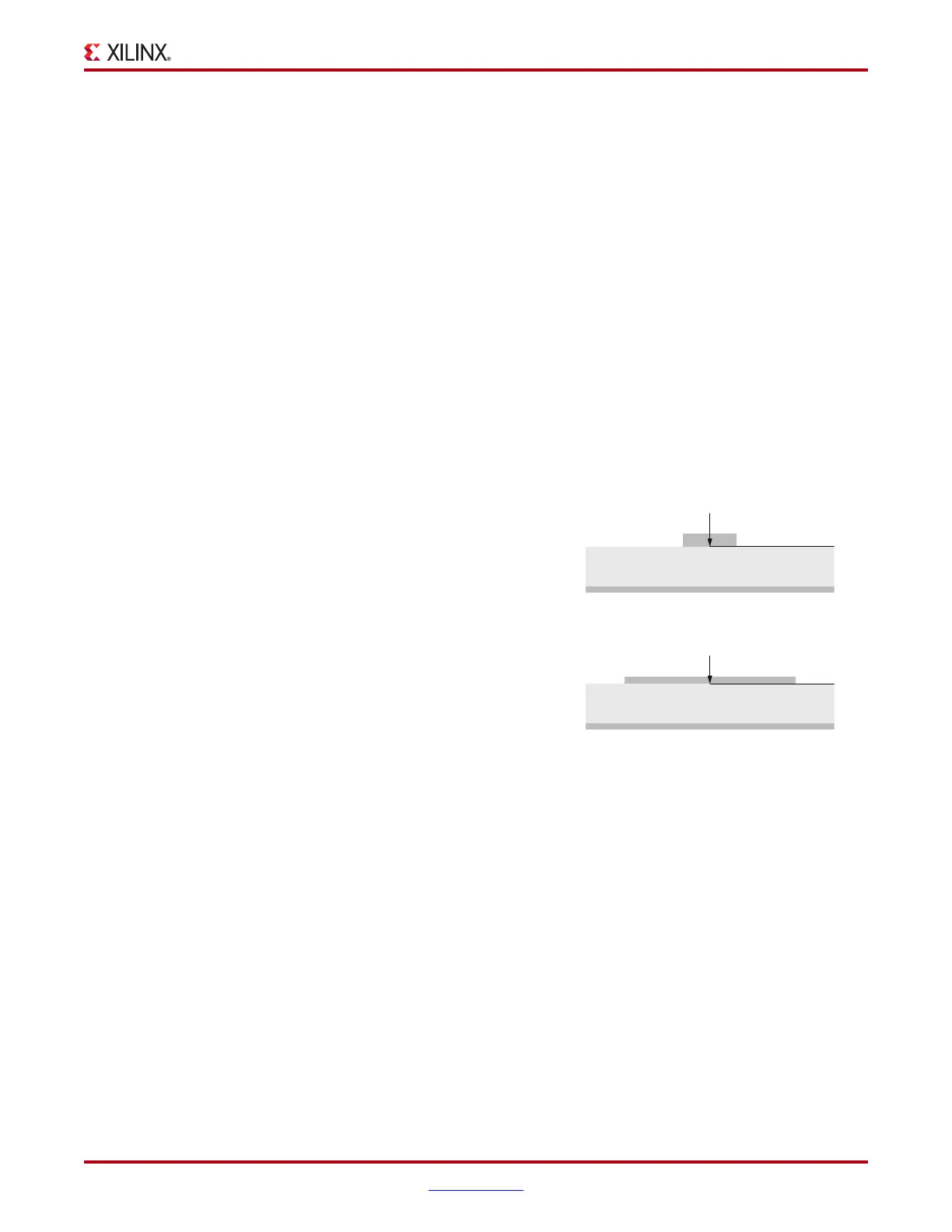
SMT Pads
For applications that require AC coupling between transmitter and receiver, SMT pads are
introduced in the channel to allow coupling capacitors to be mounted. Standard SMT pads
have excess capacitance due to plate capacitance to a nearby reference plane. In the
Figure 5-4 example, a 5 mil trace with a Z
0
of 50Ω transitions to an 0402 SMT pad that is
28 mils wide, all over 3 mils of FR4.
Using a 2D field solver on these dimensions yields a Z
0
of 50Ω for the 5 mil trace. The Z
0
for
the 0402 pad is 16Ω because the pad has too much capacitance and too little inductance,
resulting in an impedance of less than 50Ω . Performance of this transition can be
optimized in one of two ways.
The first method makes the trace the same width as the pad and moves the ground plane
deeper into the stackup to maintain the Z
0
of the transition at 50Ω. This method does not
require any special analysis, but there might be some error due to the fringing capacitance
of the SMT capacitor body. Trace density is limited because traces are now 28 mils wide.
The second method, shown in Figure 5-5, clears the ground plane underneath the pad,
which removes much of the excess capacitance caused by the plate capacitance between
the pad and the ground plane. This technique allows for greater trace density than the first
method, but requires 3D field-solver analysis or measurement along with several board
iterations to get the desired performance.
X-Ref Target - Figure 5-4
Figure 5-4: 2D Field-Solver Analysis of 5 Mil Trace and 28 Mil Pad
Line
- 5.2 mils wide over 3 mil FR4 Dielectric
- L = 288 nH/m
- C = 116 pF/m
- Zo = 50Ω
5 Mil Trace
Pad
- 28 mils wide over 3 mil FR4
- L = 98 nH/m
- C = 404 pF/m
- Zo = 16Ω
28 Mil Pad
UG393_c5_04_091809

 Loading...


