Spartan-6 FPGA PCB Design and Pin Planning www.xilinx.com 25
UG393 (v1.1) April 29, 2010
Basic PDS Principles
A connecting trace length has a large impact on the mounting’s parasitic inductance and if
used, should be as short and wide as possible. When possible, a connecting trace should
not be used (Figure 2-1A) and the via should butt up against the land (Figure 2-1B).
Placing vias to the side of the capacitor lands (Figure 2-1C) or doubling the number of vias
(Figure 2-1D), further reduces the mounting’s parasitic inductance.
Some PCB manufacturing processes allow via-in-pad geometries, an option for reducing
parasitic inductance. Using multiple vias per land is important with ultra-low inductance
capacitors, such as reverse aspect ratio capacitors that place wide terminals on the sides of
the capacitor body instead of the ends.
PCB layout engineers often try to squeeze more parts into a small area by sharing vias
among multiple capacitors. This technique should not be used under any circumstances. PDS
improvement is very small when a second capacitor is connected to an existing capacitor’s
vias. For a larger improvement, reduce the total number of capacitors and maintain a one-
to-one ratio of lands to vias.
The capacitor mounting (lands, traces, and vias) typically contributes about the same
amount or more inductance than the capacitor's own parasitic self-inductance.
Plane Inductance
Some inductance is associated with the PCB power and ground planes. The geometry of
these planes determines their inductance.
Current spreads out as it flows from one point to another (due to a property similar to skin
effect) in the power and ground planes. Inductance in planes can be described as spreading
inductance and is specified in units of henries per square. The square is dimensionless; the
shape of a section of a plane, not the size, determines the amount of inductance.
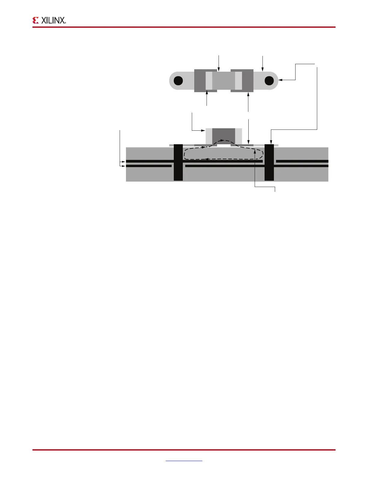
X-Ref Target - Figure 2-7
Figure 2-7: Example Cutaway View of PCB with Capacitor Mounting
Solderable End Terminal
0402 Capacitor Body
Surface Trace
Capacitor Solder Land
Via
PCB
GND
V
CC
Power and
Ground Planes
Mounted Capacitor Current Loop
UG393_c2_07_091809

 Loading...


