22 www.xilinx.com Spartan-6 FPGA PCB Design and Pin Planning
UG393 (v1.1) April 29, 2010
Chapter 2: Power Distribution System
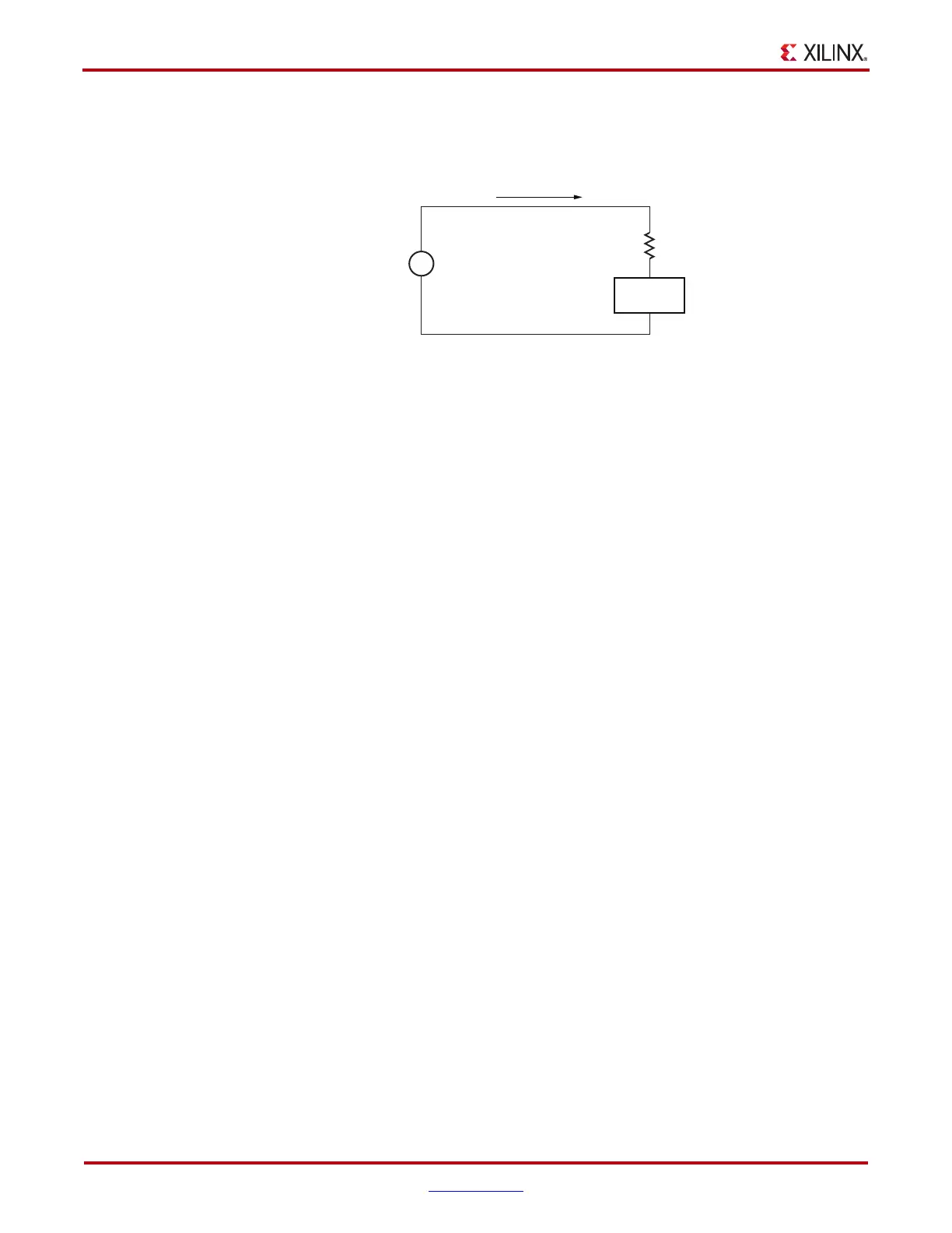
Figure 2-4 shows a simplified PDS circuit with all reactive components represented by a
frequency-dependent resistor.
Role of Inductance
Inductance is the property of the capacitors and the PCB current paths that slows down
changes in current flow. Inductance is the reason why capacitors cannot respond
instantaneously to transient currents or to changes that occur at frequencies higher than
their effective range.
Inductance can be thought of as the momentum of charge. Charge moving through a
conductor represents some amount of current. If the level of current changes, the charge
moves at a different rate. Because momentum (stored magnetic-field energy) is associated
with this charge, some amount of time and energy is required to slow down or speed up
the charge flow. The greater the inductance, the greater the resistance to change, and the
longer the time required for the current level to change. A voltage develops across the
inductance as this change occurs.
The PDS, made up of a regulator and multiple stages of decoupling capacitors,
accommodates the device current demand and responds to current transients as quickly as
possible. When these current demands are not met, the voltage across the device's power
supply changes. This is observed as noise. Inductance in the current path of the capacitors
should be minimized, because it retards the ability of decoupling capacitors to quickly
respond to changing current demands.
Inductances occur between the FPGA device and capacitors and between the capacitors
and the voltage regulator (see Figure 2-3). These inductances occur as parasitics in the
capacitors and in all PCB current paths. It is important that each of these parasitics be
minimized.
Capacitor Parasitic Inductance
The capacitance value is often considered the bypass capacitors’s most important
characteristic. In power system applications, the parasitic inductance (ESL) has the same or
greater importance. Capacitor package dimensions (body size) determine the amount of
parasitic inductance. Physically small capacitors usually have lower parasitic inductance
than physically large capacitors.
X-Ref Target - Figure 2-4
Figure 2-4: Further Simplified PDS Circuit
l
TRANSIENT
FPGA
ug393_c2_04_091809
Z
P
(f)
V
RIPPLE
+
−
+
V

 Loading...


