24 www.xilinx.com Spartan-6 FPGA PCB Design and Pin Planning
UG393 (v1.1) April 29, 2010
Chapter 2: Power Distribution System
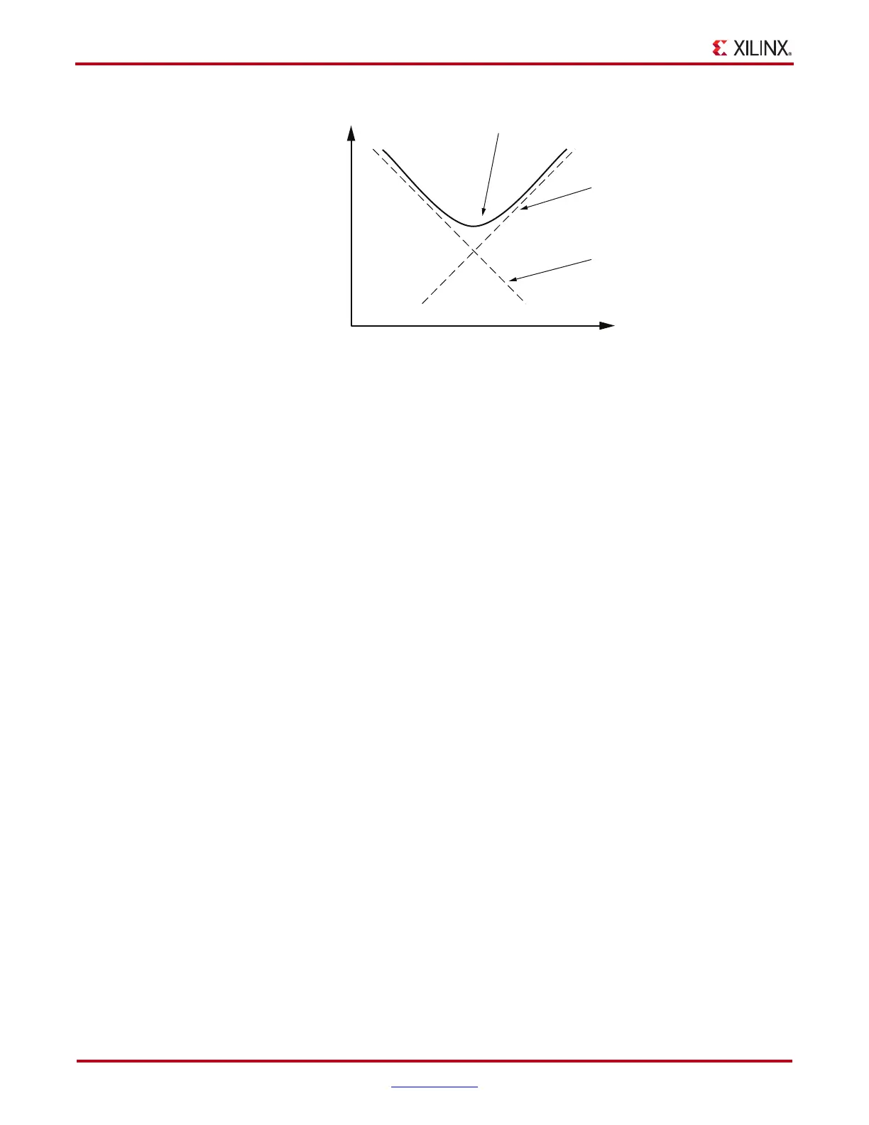
As capacitive value is increased, the capacitive curve moves down and left. As parasitic
inductance is decreased, the inductive curve moves down and right. Because parasitic
inductance for capacitors in a specific package is fixed, the inductance curve for capacitors
in a specific package remains fixed.
As different capacitor values are selected in the same package, the capacitive curve moves
up and down against the fixed inductance curve, as shown in Figure 2-8.
The low-frequency capacitor impedance can be reduced by increasing the value of the
capacitor; the high-frequency impedance can be reduced by decreasing the inductance of
the capacitor. While it might be possible to specify a higher capacitance value in the fixed
package, it is not possible to lower the inductance of the capacitor (in the fixed package)
without putting more capacitors in parallel. Using multiple capacitors in parallel divides
the parasitic inductance, and at the same time, multiplies the capacitance value. This
lowers both the high and low frequency impedance at the same time.
PCB Current Path Inductance
The parasitic inductance of current paths in the PCB have three distinct sources:
•Capacitor mounting
• PCB power and ground planes
•FPGA mounting
Capacitor Mounting Inductance
Capacitor mounting refers to the capacitor's solder lands on the PCB, the trace (if any)
between the land and via, and the via.
The vias, traces, and capacitor mounting pads of a 2-terminal capacitor contribute
inductance between 300 pH to 4 nH depending on the specific geometry.
Because the current path’s inductance is proportional to the loop area the current traverses,
it is important to minimize this loop size. The loop consists of the path through one power
plane, up through one via, through the connecting trace to the land, through the capacitor,
through the other land and connecting trace, down through the other via, and into the
other plane, as shown in Figure 2-7.
X-Ref Target - Figure 2-6
Figure 2-6: Contribution of Parasitics to Total Impedance Characteristics
Frequency
Impedance
Capacitive
Contribution (C)
Inductive
Contribution (ESL)
To tal Impedance Characteristic
ug393_c2_06_091809

 Loading...


