48 www.xilinx.com Spartan-6 FPGA PCB Design and Pin Planning
UG393 (v1.1) April 29, 2010
Chapter 5: Design of Transitions for High-Speed Signals
The magnitude of this excess capacitance (C) or inductance (L) can also be extracted from
the TDR waveform by integrating the normalized area of the transition’s TDR response.
The respective equations for capacitance and inductance are:
Equation 5-1
Equation 5-2
Figure 5-3 shows the integration of the normalized TDR area.
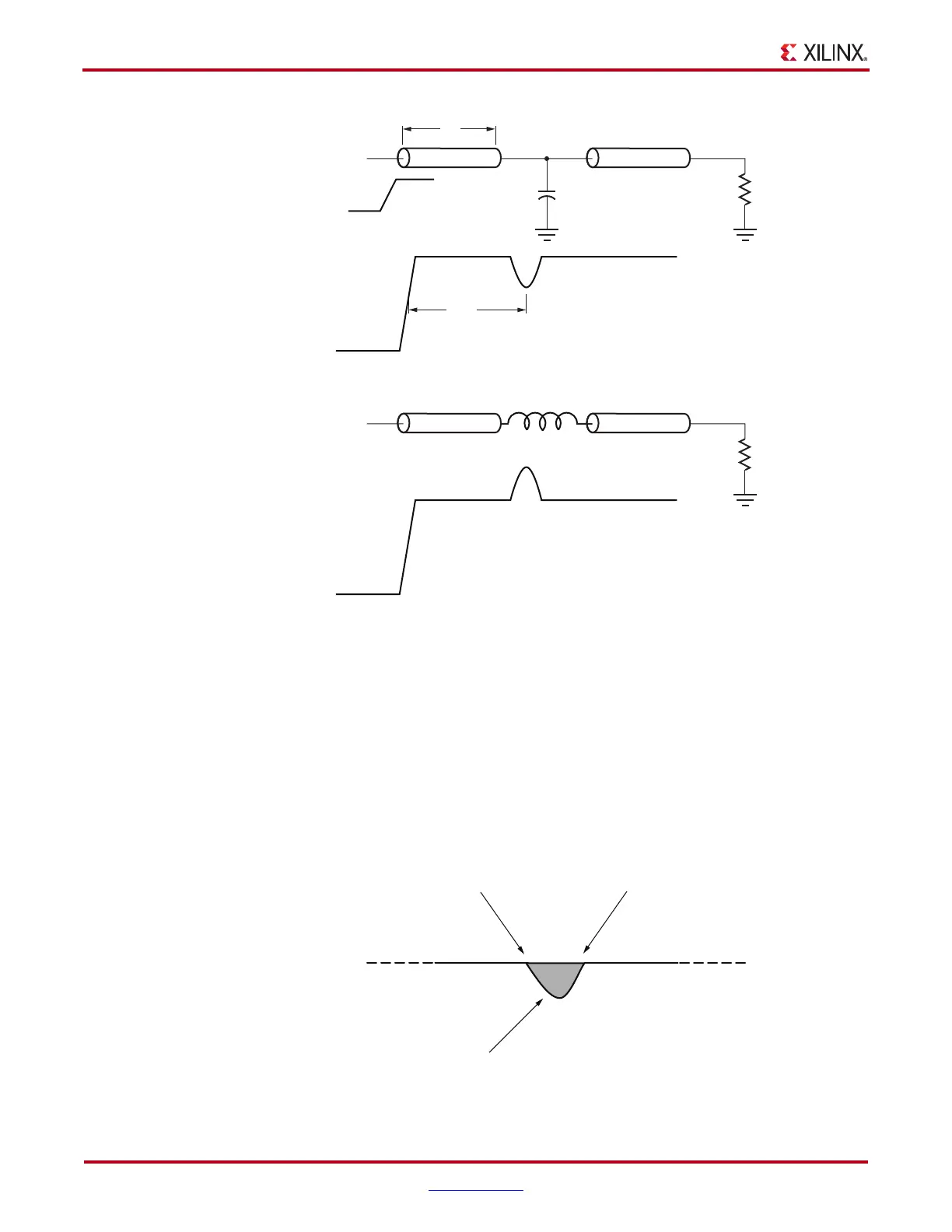
X-Ref Target - Figure 5-1
Figure 5-1: TDR Signature of Shunt Capacitance
X-Ref Target - Figure 5-2
Figure 5-2: TDR Signature of Series Inductance
X-Ref Target - Figure 5-3
Figure 5-3: Integration of Normalized TDR Area
Td
2Td
C50Ω
UG393_c5_01_091809
50Ω
UG393_c5_02_091809
C
2
Z
0
------–
V
tdr
t() V
step
–
V
step
-------------------------------------
dt
t1
t2
∫
=
L 2Z
0
V
tdr
t() V
step
–
V
step
-------------------------------------
dt
t1
t2
∫
=
t
2
Shaded area goes into the
integral for Equation 13-2
UG393_c5_03_091809
t
1

 Loading...


