60 YASKAWA ELECTRIC EZZ010928 FSDrive-MV1000 Instructions
3.4 Routing Cables
3.4 Routing Cables
The structure of the terminals conforms to JCS standards stipulated by the Japanese Electric Wire & Cable Makers’
Association. Route the cables according to the JCS standards appropriate for the input voltage used.
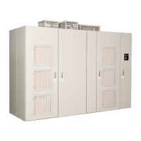
Examples of cable routing are shown below.
Note: Secure the cables with cable brackets. Do not secure them at an intermediate point between the cable bracket and control circuit
terminals. Prepare cable brackets suitable for the size of the cables used.
◆ Check Before Routing Cables
■ Main Circuit Input-side Cable
Route the input cable at the input side of the drive into the transformer panel through the inlet port of the drive input
cable at the bottom of the transformer panel.
Mount a cable bracket on the cable bracket clamp near the cable inlet port to secure the cables.
■
Main Circuit Output-side Cable
Route the output cable at the output side of the drive into the Power Cell panel through the inlet port of the drive output
cable at the bottom of the transformer panel.
Mount a cable bracket on the cable bracket clamp near the cable inlet port to secure the cables.
NOTICE: Keep the wiring for the main circuit separate from that for the control circuit. Select a power supply with a capacity larger
than that of the drive to be connected. When connecting multiple drives to a single power supply, select a power supply with
a capacity larger than the sum of the power required by all the drives to be connected. Even when the power supply has
sufficient capacity, the power supply voltage may drop when the power is turned on, causing malfunction of connected
devices if the power supply has a large power impedance.
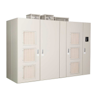
Figure 3. 5
Figure 3.5 Cable Routing (Drive: 2-kV Class, 700 HP)
A – Cooling fan E – Cable bracket clamp
B – Power Cell F – Main circuit cable
C – Control circuit terminal G – Cable bracket
D – Main circuit output terminals U, V and W H – Main circuit input terminals R, S, and T
Transformer panel
Left side view
Power Cell panel
Front view
Right side view
Control panel
A
B
F
G
D
C
F
E
H
FF
G
E
%$
(.
$0.$0.
$0.$0.
%$
%$
$0.$0.
$0.$0.
%$
$0.$0.
$0.$0.
$0.$0.
$0.$0.
ᵈᗧᵈᗧᵈᗧ
ᵈᗧᵈᗧᵈᗧ
%#76+10
2NGCUGNCRDCPFDGVYGGPRCPGNHNCOG
%#76+10
DGVYGGPRCPGNHNCOGCPFVJKUWPKV
2NGCUGFQPQVECVEJVJGHKPIGT
JQNGCPFJCPFNGCVVTCPURQTV
ޓࡄࡀ࡞ࡈ㧙ࡓߣᧄ࡙࠾࠶࠻ߣߩ㑆ߢᜰࠍ߹ߥࠃ߁ߦ
ޓャㅍᤨߩࡂࡦ࠼࡞ᛮߌ㒐ᱛ↪ߦࡄࡀ࡞ࡈ㧙ࡓⓣߣࡂࡦ࠼࡞
ߩ㑆ߦ⚿᧤ࡃࡦ࠼╬ࠍᏎ߈ઃߌߡߐޕ
%%
%%
66
66
66
66
%%
%%
66
66
66
66
%%
%%
66
66
66
66
'&'&
$0.$0.
$0.$0.
5%5%
4%4%
'&'&
'&'&
'&'&
'&'&
'&'&
'&'&
'&'&
'&'&
'&'&
'&'&
..
..
..
..
..
..
..
..
..
$0.$0.
(.
'&'&
$0.$0.
$0.$0.
5%5%
4%4%
'&'&
'&'&
'&'&
'&'&
'&'&
'&'&
'&'&
'&'&
'&'&
'&'&
..
..
..
..
..
..
..
..
..
$0.$0.
㨀㧛㨀㧛 㧿㧛㧿㧛
㨁㧝㨁㧝
㧱㧭㧱㧭
㨂㧝㨂㧝
㧾㧛㧾㧛
㧱㧭㧱㧭
㨃㧝㨃㧝
㧱㧭㧱㧭
V
U
W
T
S
R
 Loading...