Note:
• "Vega 10" supports ×16 lane reversal, where the receivers on lanes 0 to 15 of
the graphics endpoint are mapped to the transmitter on lanes 15 down to 0 of
the root complex. If ×16 lane reversal is employed, both the receive and
transmit lanes must be reversed. In addition, polarity inversion is supported,
such as when the + of the differential pair is connected to the - at the root
complex.
• 220-nF AC-coupling capacitors are required.
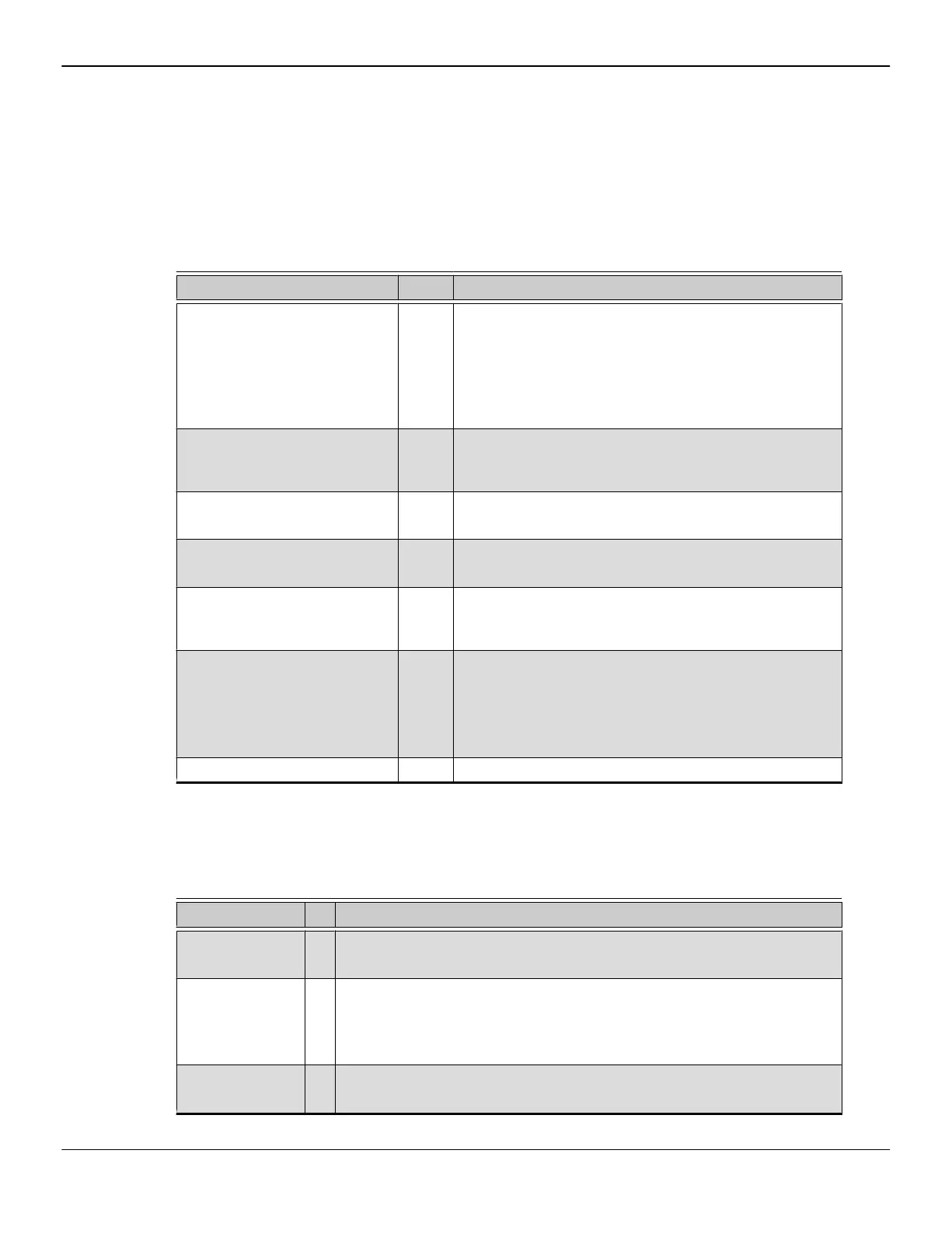
Table 3–3 PCI Express® Bus Interface
Pin Name I/O Description
PERSTB I
Fundamental reset.
3.3-V tolerant pad.
This signal must be asserted during any fundamental reset
event, such as power up, warm boot, reset button pressed,
CTL-ALT-DEL, Windows restart, or wake from D3.
A buffered reset signal dedicated to the GPU is required.
PCIE_REFCLKP/N I
PCI Express PLL differential reference clock (+/-).
100-MHz (± 300 ppm) input frequency; 0-V to 0.7-V single-
ended swing.
PCIE_TX[15:0]P/N O
PCI Express transmitter output data channel TX[15:0] (+/-).
Differential serial data transmitted up to 8.0-GT/s bit rate.
PCIE_RX[15:0]P/N I
PCI Express receiver input data channel RX[15:0] (+/-).
Differential serial data received up to 8.0-GT/s bit rate.
PCIE_ZVSS I/O
Connect to VSS through a 200-Ω (1% tolerance) 100 ppm/C
resistor.
Resistor parasitic capacitance <10 pF.
CLKREQB I/O
CLKREQB only: CLKREQB is an open drain output from the
GPU and an input to the platform which can be used to
request the PCIe® reference clock to GPU on or off.
L1 PM Substates: CLKREQB is a bi-directional open drain
that can be asserted by either the GPU or the platform to
initiate an L1 exit.
WAKEB I Reserved. Do not connect on the PCB.
3.3 Memory Interface (HBM)
Table 3–4 Memory Interface
Pin Name I/O Description
HBMA_DAP_[0:59]
HBMB_DAP_[0:59]
I/O Debugging purposes, can be left floating.
VREFEXTA
VREFEXTB
I/O
External voltage reference for HBM.
0.5 × VDDIO_MEM
Two 100-Ω 1% resistors can be used to form the divider on each pin. Filter
capacitor is needed to ensure AC noise is within ±10 mV.
MTESTA
MTESTB
O Reserved. Provide test pads on the PCB.
22 Signal Descriptions
"Vega 10" Databook
56006_1.00
© 2017 Advanced Micro Devices, Inc.
AMD Confidential - Do not duplicate.