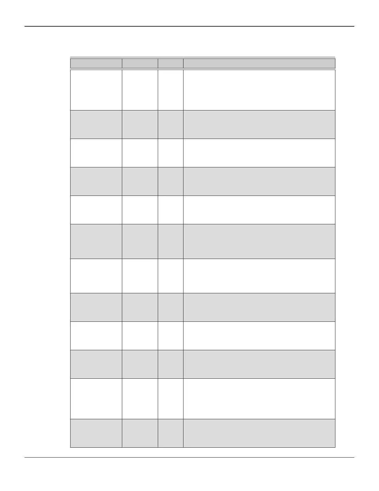
3.9 General Purpose I/O Interface
Table 3–10 General Purpose I/O Interface
Pin Name Type PD/PU Description
GPIO_0 I/O
3.3V
(VDDAN_33)
PD-reset General purpose I/O.
Can be used as interrupt input to trigger fast power
reduction from GPU when system power source is switched
from AC adapter to battery.
Can be left unconnected if not used.
GPIO_1 I/O
3.3V
(VDDAN_33)
PD-reset General purpose I/O.
Can be unconnected if not used.
GPIO_2 I/O
3.3V
(VDDAN_33)
PD-reset General purpose I/O.
Can be unconnected if not used.
GPIO_3 I/O
3.3V
(VDDAN_33)
PD-reset General purpose I/O.
Can be unconnected if not used.
GPIO_4 I/O
3.3V
(VDDAN_33)
PD-reset General purpose I/O.
Can be unconnected if not used.
GPIO_5 I/O
3.3V
(VDDAN_33)
PD-reset General purpose I/O.
Can be used as VRHOT interrupt to the GPU indicating
thermal overload of the regulator.
Can be unconnected if not used.
GPIO_6 I/O
3.3V
(VDDAN_33)
PD-reset General purpose I/O.
Can be used as an alternative input for VRHOT interrupt to
the GPU indicating thermal overload of the regulator.
Can be unconnected if not used.
GPIO_7_ROMSCK I/O
3.3V
(VDDAN_33)
PD-reset For designs that have dedicated ROM for video BIOS, it
serves as the serial ROM clock.
See Table 3–9 (p. 26) for serial ROM usage.
GPIO_8_ROMSI I/O
3.3V
(VDDAN_33)
PD-reset For designs that have dedicated ROM for video BIOS, it
serves as the serial ROM input.
See Table 3–9 (p. 26) for serial ROM usage.
GPIO_9_ROMSO I/O
3.3V
(VDDAN_33)
PD-reset For designs that have dedicated ROM for video BIOS, it
serves as the serial ROM output.
See Table 3–9 (p. 26) for serial ROM usage.
GPIO_10_ROMCSB I/O
3.3V
(VDDAN_33)
PU-reset For designs that have dedicated ROM for video BIOS, it
serves as the serial ROM chip-select. See Table 3–9 (p.
26) for serial ROM usage.
Also serves as pin strap.
See Table 3–24 (p. 38) for pin strap definition.
GPIO_11 I/O
3.3V
(VDDAN_33)
PD-reset General purpose I/O and pin strap.
See Table 3–24 (p. 38) for pin strap definition.
Signal Descriptions 27
© 2017 Advanced Micro Devices, Inc.
AMD Confidential - Do not duplicate.
"Vega 10" Databook
56006_1.00