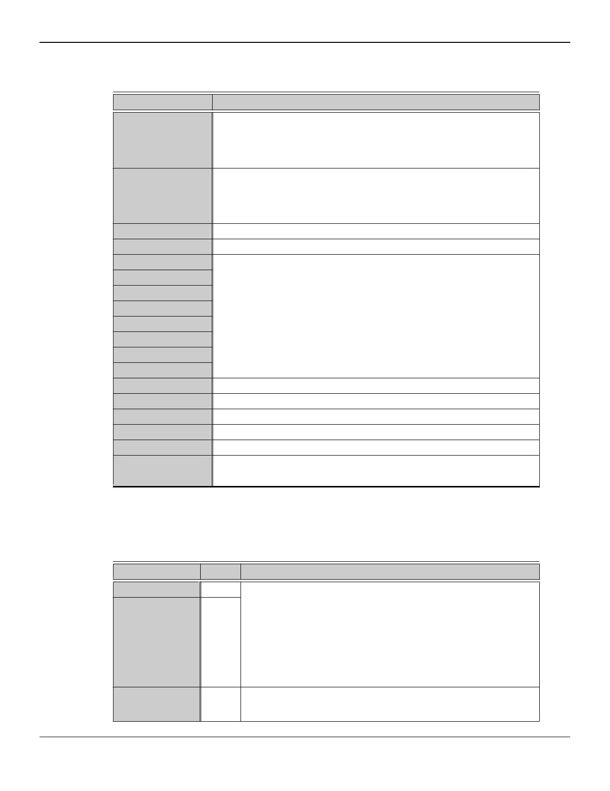
3.15 Debug Port
Table 3–16 Debug Port
Pin Name Functional Name
SMBCLK
SMBus clock.
Connected to the SMBCLK line of the SMBus master with an external pull-up
resistor to 3.3 V.
Supports the SMBus 2.0 protocol.
SMBDAT
SMBus data.
Connected to the SMBDAT line of the SMBus master with an external pull-up
resistor to 3.3 V.
Supports the SMBus 2.0 protocol.
TEST6
Connect to ground through a 0-Ω resistor on the PCB.
BP_[0:3]
Connect to 1.8 V through pull-up resistors on the PCB.
INTCRACKMONDA
Not connected on the PCB.
INTCRACKMONDB
INTCRACKMONGLL
INTCRACKMONGLR
INTCRACKMONGUL
INTCRACKMONGUR
INTCRACKMONP
INTCRACKMONPDG
XTRIG6
Provide a pull-up resistor footprint to 1.8 V on the PCB.
XTRIG7
Provide a pull-up resistor footprint to 1.8 V on the PCB.
ANALOGIO
Provide access on the PCB through a test pad.
PINSTRAP_[0:7]
Debug bus output data.
DFTIO_ [0:383]
Not connected on the PCB.
PLLCHARZ1_L
PLLCHARZ1_H
Each of the two balls should be connected to a capacitor (0.1 µF) in series with
a resistor (51.1 Ω) to ground.
3.16 Thermal Information and Management Interface
Table 3–17 Thermal Interface Signals
Pin Name Type Description
DPLUS
Anode DPLUS: Thermal diode plus side (anode), used by the external
temperature controller to obtain GPU die temperature.
DMINUS: Thermal diode minus side (cathode), used by the external
temperature controller to obtain the GPU die temperature.
Note: Can be unconnected if not used.
DPLUS and DMINUS routing must have minimum resistance; less than
0.02Ω. Routed as differential pair, referencing to ground with minimal
plane crossings, and kept away from high speed signals.
DMINUS
Cathode
TEMPIN
1
I
TEMPIN: A provision to connect to the anode of an external thermal diode
(or base and collector of NPN transistor) for the GPU to read the
temperature from a spot of interest on the board or platform.
Signal Descriptions 33
© 2017 Advanced Micro Devices, Inc.
AMD Confidential - Do not duplicate.
"Vega 10" Databook
56006_1.00