8
Boundary Scan Specification
This chapter contains information on boundary scan specifications as they apply to
"Vega 10". To go to a topic of interest, use the following list of linked cross-references:
• Introduction (p. 77)
• Boundary Scan (p. 77)
• JTAG Interface Signals (p. 77)
• JTAG Timing Characteristics (p. 78)
8.1 Introduction
"Vega 10" has a JTAG 1149.1 compliant TAP controller. The boundary scan implementation is
IEEE compliant. The implementation supports BYPASS, EXTEST, and PRELOAD instructions.
A BSDL file for each of the modes can be obtained from the AMD OEM Resource Center.
8.2 Boundary Scan
The "Vega 10" boundary scan can perform board-level capture and drive out on all
pins mentioned in the BSDL file.
8.3 JTAG Interface Signals
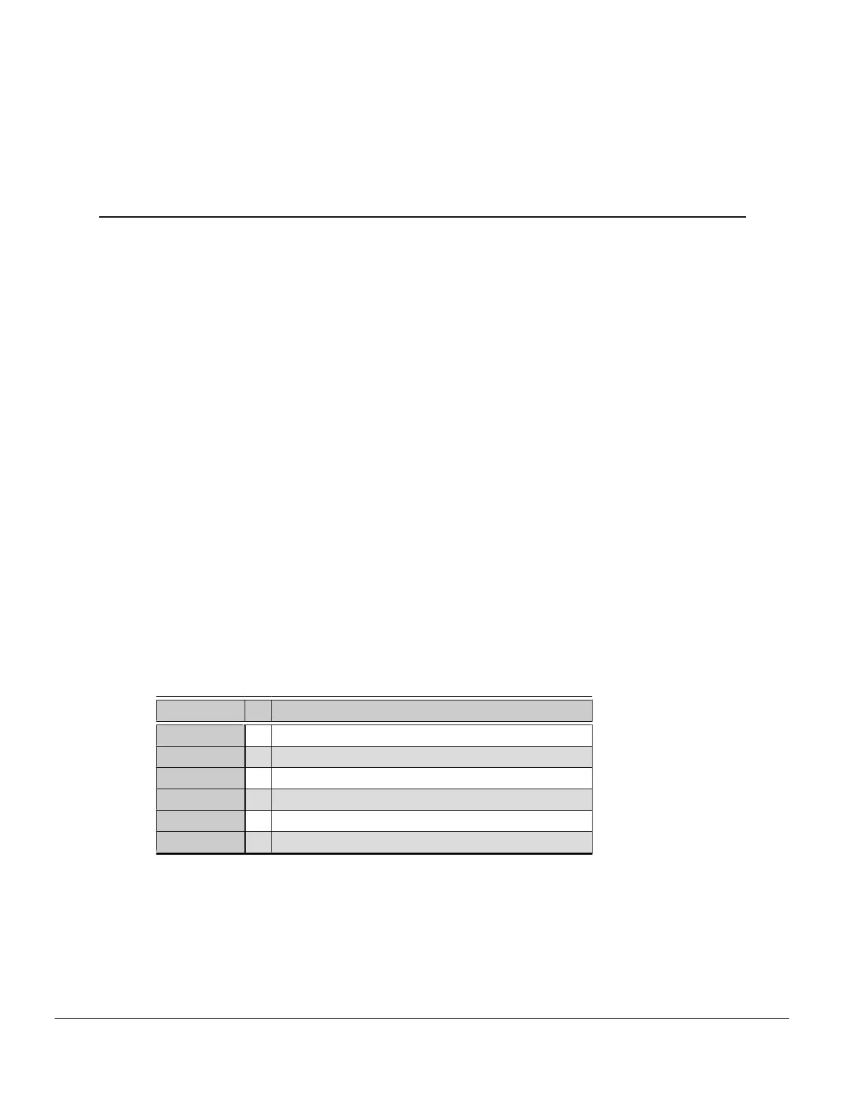
Table 8–1 JTAG Interface
Pin-name I/O Description
JTAG_TCK
I TCK: Test clock.
JTAG_TMS
I TMS: Test mode select.
JTAG_TDI
I TDI: Test data in.
JTAG_TDO
O TDO: Test data out.
JTAG_TRSTB
I TRST#: Test asynchronous reset.
TESTEN
I Compliance pin: Pull up to 3.3 V to enable JTAG access.
© 2017 Advanced Micro Devices, Inc.
AMD Confidential - Do not duplicate.
"Vega 10" Databook
56006_1.00