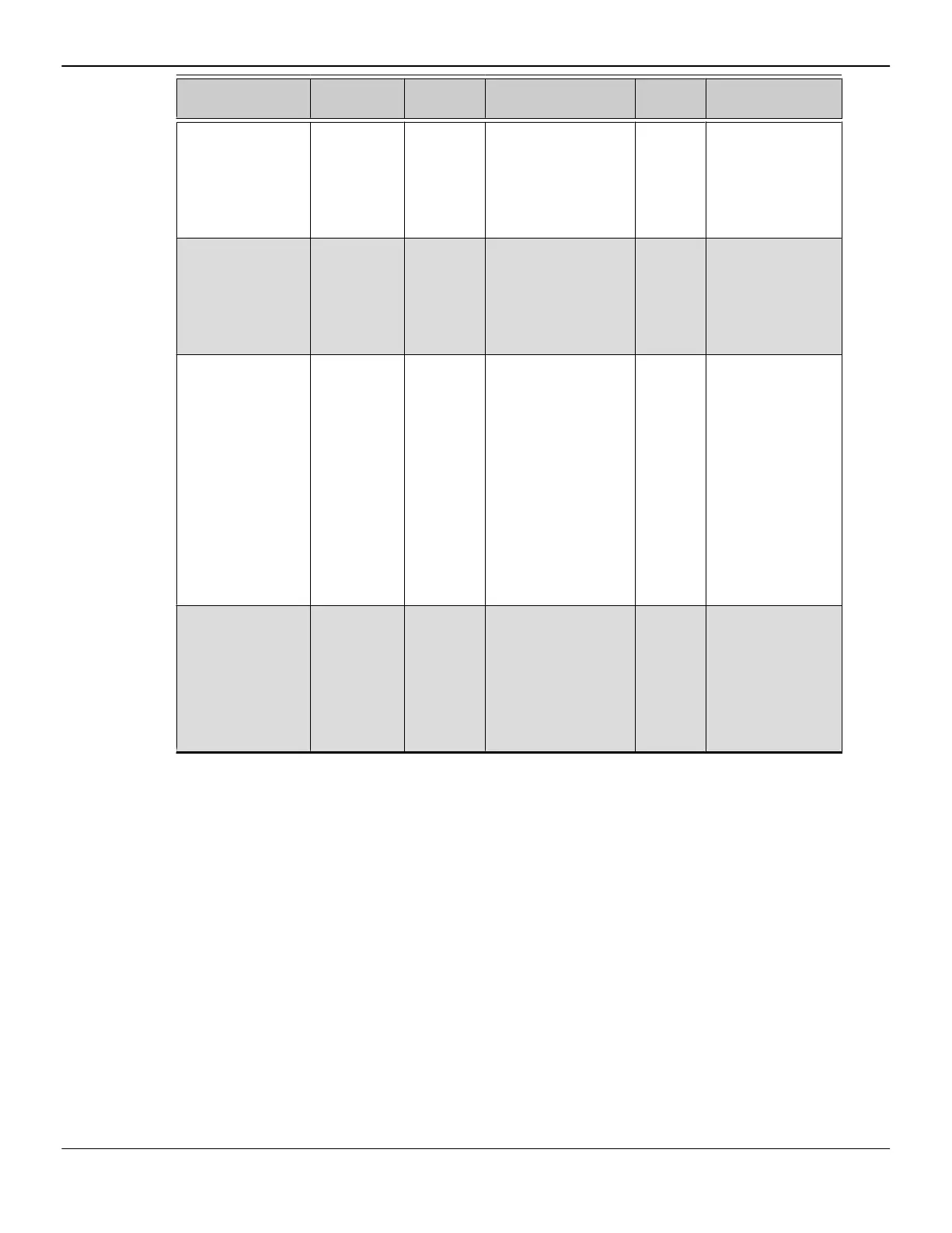
Strap Name Pin Name Power
Rail
Description GPU
Default
Recommended
Settings
1
SMBUS_ADDR GPIO_19 VDDAN_33 Provide a strap option
to change the SMBUS
slave address of the
GPU.
0: 0×41
1: 0×40
0
(Internal
pull-
down)
Design dependent.
Provide a pull-up
resistor option to
VDDAN_33 on the
PCB for the pin.
BIF_GEN3_DIS_A PINSTRAP_6 VDDAN_18 Disable/Enable PCIe
Gen3 capability.
0: PCIe Gen3 is
supported.
1: PCIe Gen3 is not
supported.
0
(Internal
pull-
down)
Design dependent.
Provide a pull-up
resistor option to
1.8 V on the PCB.
BIF_CLK_PM_EN PINSTRAP_7 VDDAN_18 Determines whether
or not the PCIe
reference clock power
management
capability is reported
in the PCI
configuration space
(otherwise known as
CLKREQB).
0: The CLKREQB
power management
capability is disabled.
1: The CLKREQB
power management
capability is enabled.
0
(Internal
pull-
down)
Design dependent.
Provide a pull-up
resistor option to
1.8 V on the PCB.
BIF_LC_TX_SWING GPIO_13 VDDAN_33 Controls the
transmitter full/
reduced swing mode.
0: The transmitter
full-swing is enabled.
1: The transmitter
reduced-swing is
enabled.
0
(Internal
pull-
down)
0
Provide a pull-up
resistor option to
VDDAN_33 on the
PCB.
3.21.2 ROM Configurations
For designs that have a dedicated ROM device for the GPU video BIOS:
• Use the GPU default strap on GPIO_10 (i.e., 1).
• Use the GPU default straps on PINSTRAP[2:0] (i.e., 101).
3.21.3 ROM Straps for Add-in Card Design
If the ROM is attached (see ROM_CONFIG[2:0] pin-based straps), after PERSTB goes
inactive (high), the ROM is read at the addresses listed below and default settings
are applied.
The ROM based straps are ORed with the pin-based straps.
40 Signal Descriptions
"Vega 10" Databook
56006_1.00
© 2017 Advanced Micro Devices, Inc.
AMD Confidential - Do not duplicate.