3.7 Hardware I
2
C Interface
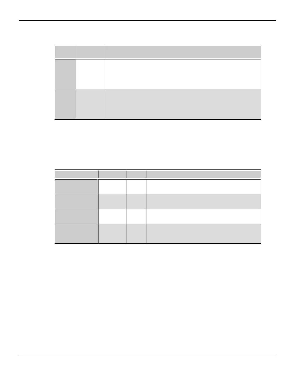
Table 3–8 Hardware IC Interface
Pin
Name
I/O Description
SCL
I/O
(VDDAN_33)
I
2
C clock.
Note: Can be left unconnected if not used.
Frequency: Up to 100 KHz I
2
C standard; Up to 400 KHz fast; and up to 1 MHz
fast mode plus.
SDA
I/O
(VDDAN_33)
I
2
C clock.
Note: Can be left unconnected if not used.
Frequency: Up to 100 KHz I
2
C standard; Up to 400 KHz fast; and up to 1 MHz
fast mode plus.
3.8 Serial Flash Interface
Configuration straps must be set to identify the appropriate ROM type. See
Configuration Straps (p. 37).
Table 3–9 Serial Flash Interface
Pin Name Type PD/PU Description
GPIO_9_ROMSO
I
(VDDAN_33)
PD-reset
Serial-ROM output from ROM.
General purpose I/O or open-drain output.
GPIO_8_ROMSI
O
(VDDAN_33)
PD-reset
Serial-ROM input to ROM.
General purpose I/O or open-drain output.
GPIO_7_ROMSCK
O
(VDDAN_33)
PD-reset
Serial-ROM clock to ROM.
General purpose I/O or open-drain output.
GPIO_10_ROMCSB
O
(VDDAN_33)
PU-reset
BIOS-ROM chip select.
Used to enable the ROM for ROM read and program
operations.
26 Signal Descriptions
"Vega 10" Databook
56006_1.00
© 2017 Advanced Micro Devices, Inc.
AMD Confidential - Do not duplicate.