5.7 DisplayPort Main Link Electrical Characteristics
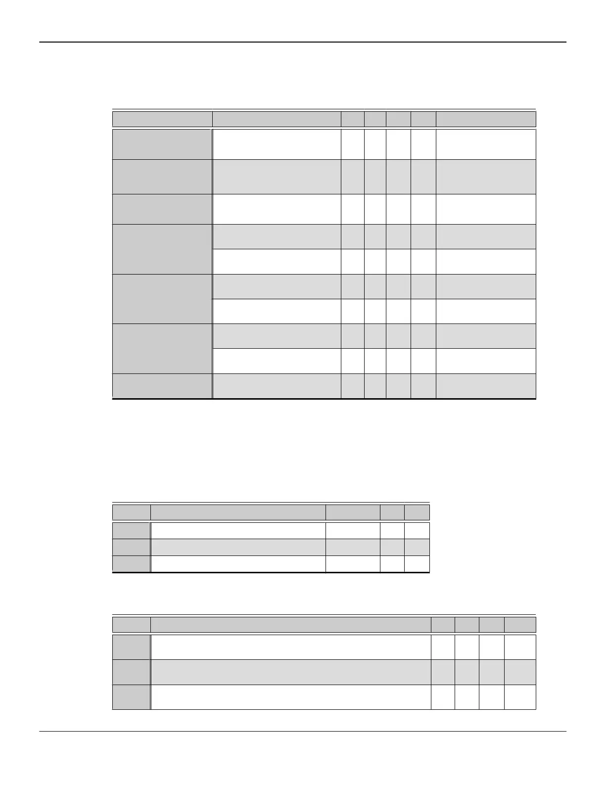
This table provides the electrical characteristics of the DisplayPort main link.
Table 5–9 DisplayPort Main Link Electrical Specification
Symbol Parameter Min Typ Max Unit Notes
UI
HIGH_RATE
Unit interval for the DP high
bit rate (2.7 Gbps/lane).
— 370 — ps
High limit = +300 ppm
Low limit = -5300 ppm
UI
LOW_RATE
Unit interval for the DP
reduced bit rate (1.62 Gbps/
lane).
— 617 — ps
High limit = +300 ppm
Low limit = -5300 ppm
UI
HIGH_RATE2
Unit interval for DP high-bit
rate 2 (5.4 Gbps/lane).
— 185 — ps
High limit = +300 ppm
Low limit = -5300 ppm
V
TX-OUTPUT-RATIO_RBR_HBR
Ratio of output voltage level 1/
level 0.
0.8 6.0 dB -
Ratio of output voltage level 2/
level 1.
0.1 5.1 dB -
V
TX-OUTPUT-RATIO_HBR2
Ratio of output voltage level 2/
level 0.
5.2 6.9 dB -
Ratio of output voltage level 2/
level 1.
1.6 3.5 dB -
V
TX-OUTPUT-RATIO_RBR_HBR
Delta of pre-emphasis level 1
versus level 0.
2.0 dB -
Delta of pre-emphasis level 2
versus level 1.
1.6 dB -
V
TX-PREEMP-OFF
Maximum pre-emphasis when
disabled.
0.25 dB -
5.8 SMBus Electrical Characteristics
The following tables provide the electrical characteristics for the SMBus DATA,
CLOCK, and CLK_REQB pads.
Table 5–10 Transmitter Electrical Specification
Symbol Description Min Max Unit
F
TX
Supported transmit data rate. — 100 kHz
V
OL
Maximum output low voltage @ I = 4 mA. — 400 mV
V
OH
Minimum output high voltage. VDD33 - 0.4 — mV
Table 5–11 Receiver Electrical Specification
Symbol Description Min Max Unit Notes
VIH
AC
Minimum AC voltage at the PAD pin that will produce a stable high
at the Y pin of the macro at FRX.
2.0 — V 3
VIL
AC
Maximum AC voltage at the PAD pin that will produce a stable low at
the Y pin of the macro.
— 0.8 V 3
VIH
DC
Minimum DC voltage at the PAD pin that will produce a stable high
at the Y pin of the macro.
2.0 — V 1
Electrical Characteristics 63
© 2017 Advanced Micro Devices, Inc.
AMD Confidential - Do not duplicate.
"Vega 10" Databook
56006_1.00

 Loading...