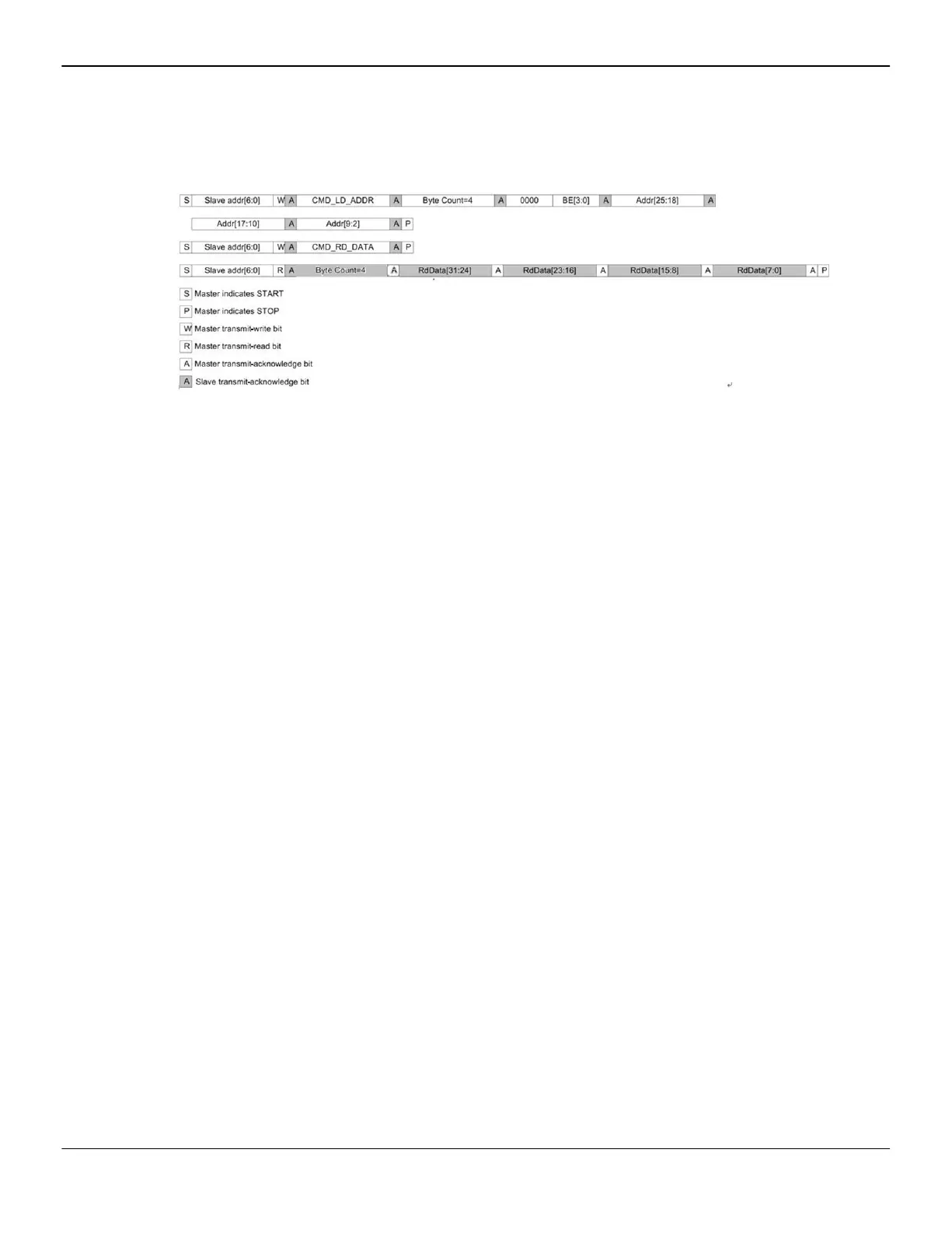
4.1.2 SMBus Read Cycle
The following figure shows an SRBM read cycle on the SMBus interface.
Figure 4–2 SMBus Read Cycle
A typical SMBus read cycle consists of the following steps:
1. Issuing a Load Address Command to the SMB_ADDR register:
a. The SMBus master issues a START bit to the slave.
b. The SMBus master issues a 7-bit slave address to the slave.
c. The SMBus master issues a write bit to the slave.
d. The SMBus slave acknowledges the master.
e. The SMBus master issues an 8-bit CMD_LD_ADDR command to the slave.
f. The SMBus slave acknowledges the master.
g. The SMBus master sends a byte count (always 4).
h. The SMBus slave acknowledges the master.
i. The SMBus master issues a 4-bit byte enable with a 4-bit zero padding.
These bits should have no effect on the reads.
j. The SMBus slave acknowledges the master.
k. The SMBus master sends SMB_ADDR[25:18] to the slave.
l. The SMBus slave acknowledges the master.
m. The SMBus master sends SMB_ADDR[17:10] to the slave.
n. The SMBus slave acknowledges the master.
o. The SMBus master sends SMB_ADDR[9:2] to the slave.
p. The SMBus slave acknowledges the master.
q. The SMBus master sends a STOP bit to the slave.
2. Issuing a Read Data Command to the slave.
a. The SMBus master issues a START bit to the slave.
b. The SMBus master issues a 7-bit slave address to the slave.
Timing Specifications 45
© 2017 Advanced Micro Devices, Inc.
AMD Confidential - Do not duplicate.
"Vega 10" Databook
56006_1.00