5.3 Power-up/down Sequence
"Vega 10" has the following requirements with regards to power-supply
sequencing to avoid damaging the GPU:
• All the GPU supplies, except for VDDAN_33, must fully reach their respective
nominal voltages within 20 ms of the start of the ramp-up sequence, though a
shorter ramp-up duration is preferred. The maximum slew rate on all rails is 50
mV/μs.
• It is recommended that the 3.3-V rail ramps up first.
• The 1.8-V rail must reach its steady state at least 10 µs before VDDCR_SOC,
VDDCR_HBM/VDDIO_MEM, VDDCI_MEM, and VDD_080/VDDCR_BACO/
VDD_080_EFUSE start to ramp up.
• VPP should reach its ready state before VDDCR_HBM/VDDIO_MEM start to
ramp.
5.4 TTL Interface Electrical Characteristics
The following table provides the electrical characteristics of the TTL Interface
(GPIOs).
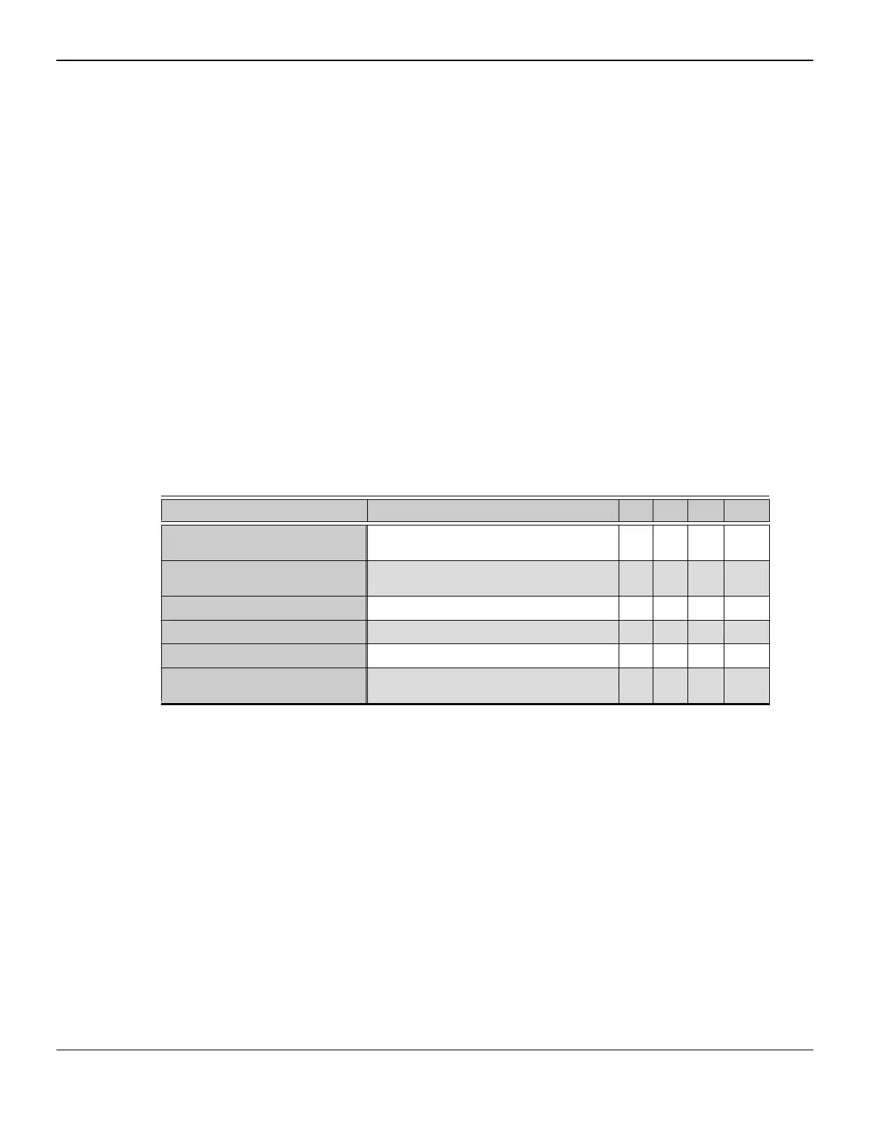
Table 5–5 DC Characteristics for 3.3-V GPIO Pads
Parameter Condition Min Max Unit Notes
V
IL
—input voltage low level.
Maximum DC voltage at the PAD pin that
will produce a logic low.
— 0.7 V —
V
IH
—input voltage high level.
Minimum DC voltage at the PAD pin that
will produce logic high.
1.7 — V —
V
OL
—output voltage low level.
Maximum output low voltage @ I = 8 mA. — 0.42 V 1, 2
V
OH
—output voltage high level.
Minimum output high voltage @ I = 8 mA. 2.5 — V 1, 2
I
OL
—output current low level.
Minimum output low current @ V = 0.1 V. 1.9 — mA 1, 2
I
OH
—output current high level.
Minimum output high current @ V =
VDDR - 0.1 V.
1.9 — mA 1, 2
5.5 DDC I
2
C Mode Electrical Characteristics
The following tables provide the electrical characteristics for the DDC pins in I
2
C
mode.
Electrical Characteristics 61
© 2017 Advanced Micro Devices, Inc.
AMD Confidential - Do not duplicate.
"Vega 10" Databook
56006_1.00