Table 4-10 SYS_CFGDATA_OUT Register bit assignments
Bits Name Function
[31:0] SYS_CFGDATA_OUT User data register output bits.
Related information
4.3 Register summary on page 4-62
4.5.4 SYS_CFGCTRL Register
The SYS_CFGCTRL Register characteristics are:
Purpose
The SYS_CFGCTRL Register controls write and read data transfer between the MCC and the
SCC interface in the FPGA.
Usage constraints
There are no usage constraints.
Configurations
Available in all MPS2 and MPS2+ configurations.
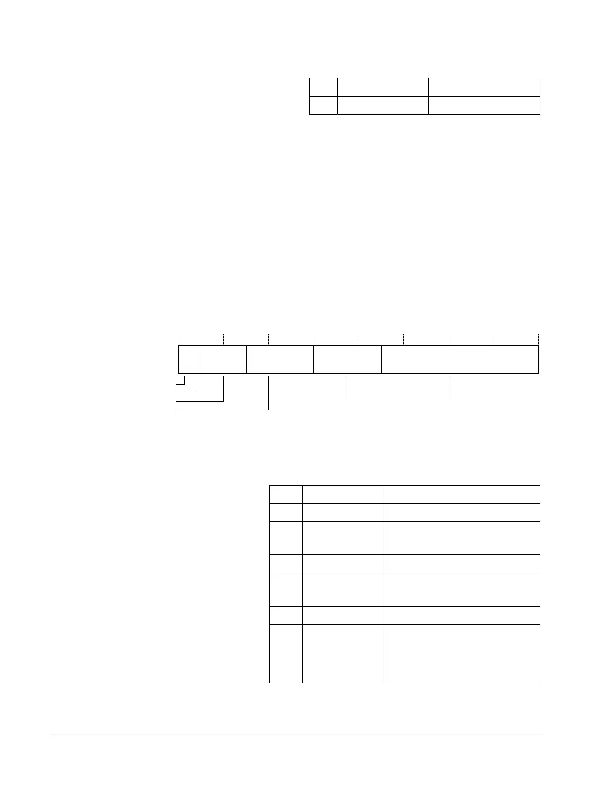
The following figure shows the bit assignments.
31
0
26 20 12
Reserved
0 0 0
0
0 0 0
30 29 25 11
Start
nRead_Write_access
Function
Reserved
0 0 0 0 0 0 0 0 0 0 0 0 0
Device
0 1
Figure 4-10 SYS_CFGCTRL Register bit assignments
The following table shows the bit assignments.
Table 4-11 SYSCFG_CTRL Register bit assignments
Bits Name Function
[31] Start Writing to this bit generates an interrupt.
[30] nRead_Write_access • 0b0 Read access
• 0b1 Write access
[29:26] - Reserved. Do not write to these bits.
[25:20] Function These bits support the following function:
• 0b000001 Clock generator
[19:12] - Reserved. Do not write to these bits.
[11:0] Device Selects device to write to or read from:
• 0x000 Clock generator 0
• 0x001 Clock generator 1
• 0x002 Clock generator 2
Related information
4.3 Register summary on page 4-62
4 Programmers Model
4.5 System configuration registers
100112_0200_09_en Copyright © 2013–2016, 2018–2020 Arm Limited or its affiliates. All
rights reserved.
4-72
Non-Confidential