Purpose
The MCC writes data to the SYS_CFGDATA_RTN Register during a read operation. This data
represents the value that the addressed MPS2 or MPS2+ FPGA Prototyping Board component
returns as a result of the read operation, for example, a clock generator frequency.
Usage constraints
The SYS_CFGDATA_RTN register is read-only to the application software in the FPGA.
Configurations
Available in all MPS2 and MPS2+ configurations.
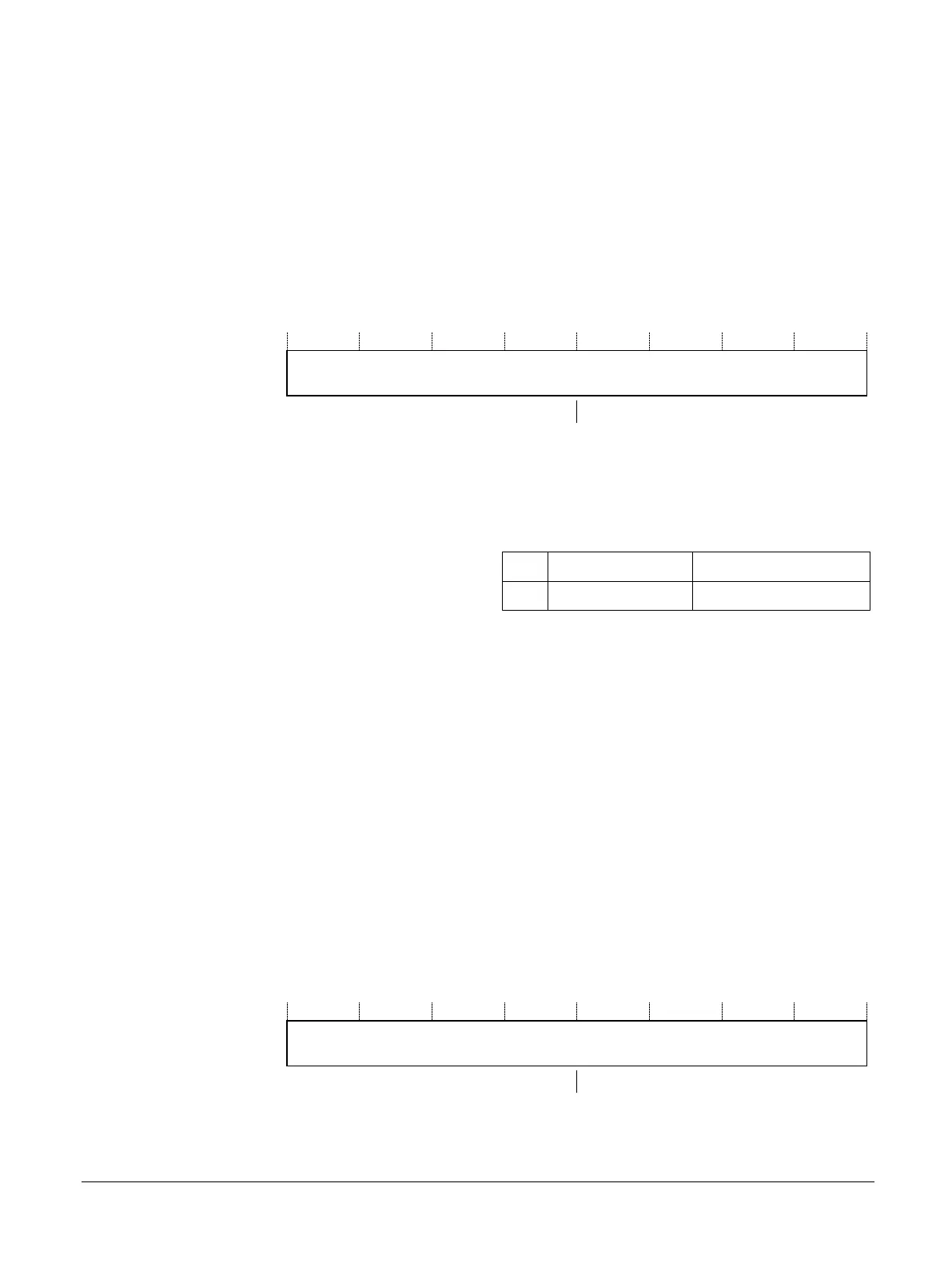
The following figure shows the bit assignments.
31
0
SYS_CFGDATA_RTN[31:0]
000000 0 0 0 0 0 0 00 0 0 0 0 0 0 00 0 0 0 0 0 0 00 0 0
Figure 4-8 SYS_CFGDATA_RTN Register bit assignments
The following table shows the bit assignments.
Table 4-9 SYS_CFGDATA_RTN Register bit assignments
Bits Name Function
[31:0] SYS_CFGDATA_RTN User data register return bits.
Related information
4.3 Register summary on page 4-62
4.5.3 SYS_CFGDATA_OUT Register
The SYS_CFGDATA_OUT Register characteristics are:
Purpose
The application software in the FPGA writes data to the SYS_CFGDATA_OUT Register during
a write operation. This data represents a value or function that the write operation sends to the
addressed MPS2 or MPS2+ FPGA Prototyping Board component, for example, a frequency
value to a clock generator.
Usage constraints
There are no usage constraints.
Configurations
Available in all MPS2 and MPS2+ Boards configurations.
The following figure shows the bit assignments.
31
0
SYS_CFGDATA_OUT[31:0]
000000 0 0 0 0 0 0 00 0 0 0 0 0 0 00 0 0 0 0 0 0 00 0 0
Figure 4-9 SYS_CFGDATA_OUT Register bit assignments
The following table shows the bit assignments.
4 Programmers Model
4.5 System configuration registers
100112_0200_09_en Copyright © 2013–2016, 2018–2020 Arm Limited or its affiliates. All
rights reserved.
4-71
Non-Confidential