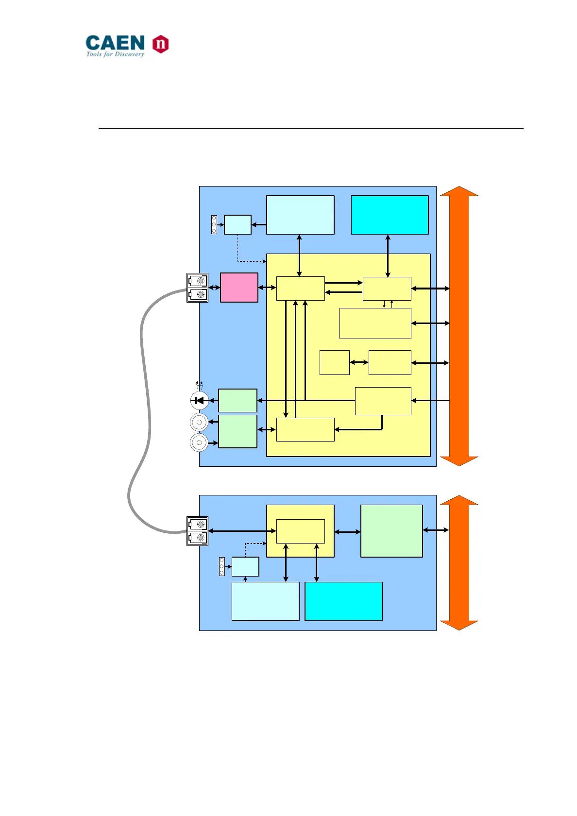
Fig. 1: Mod. V2718 block diagram
The FPGA (Field Programmable Gate Array) is the module’s core; it implements the
CONET communication protocol, the LED display and I/O connectors management on
the front side and the VME Master on the backside.
A 128 kbyte buffer allows to provide a temporary data storage during VME cycles: the
VME data rate is thus decoupled from the PCI rate and may take place at full speed.