Mod. V2718 VME PCI Optical Link Bridge
2.13.26. Display Data High register
(Base Address + 0x23, D16, read only)
This register allows to monitor the LED Display Data bits[31..16].
15 14 13 12 11 10 9 8 7 6 5 4 3 2 1 0
DISP_DATA[31:16]
Fig. 29: Display Data High register
2.13.27. Display Control Left register
(Base Address + 0x24, D16, read only)
This register allows to monitor the LED Display Control Left bar.
15 14 13 12 11 10 9 8 7 6 5 4 3 2 1 0
AM[5:0]
DS0
DS1
AS
IACK
WR
LWRD
Fig. 30: Display Control Left register
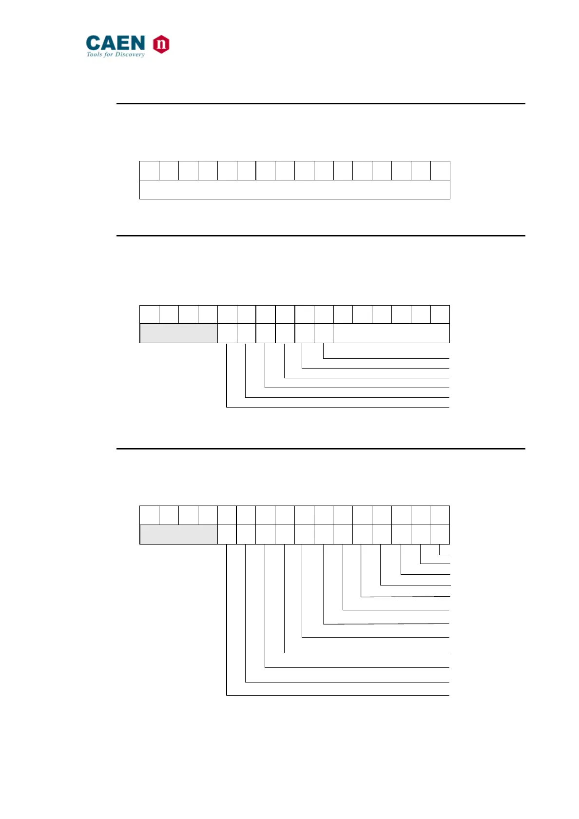
2.13.28. Display Control Right register
(Base Address + 0x25, D16, read only)
This register allows to monitor the LED Display Control Left bar.
15 14 13 12 11 10 9 8 7 6 5 4 3 2 1 0
IRQ1
IRQ2
IRQ3
IRQ4
IRQ5
IRQ6
IRQ7
BRQ
BGR
SRES
DTK
BERR
Fig. 31: Display Control Left register