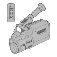
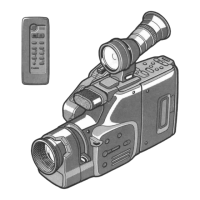
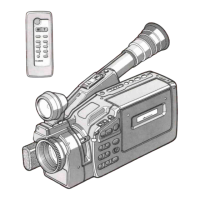
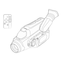
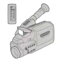
MV750i E, MV730i E, MV700i E, MV700 E, MV690 E
TECHNICAL DESCRIPTION
6
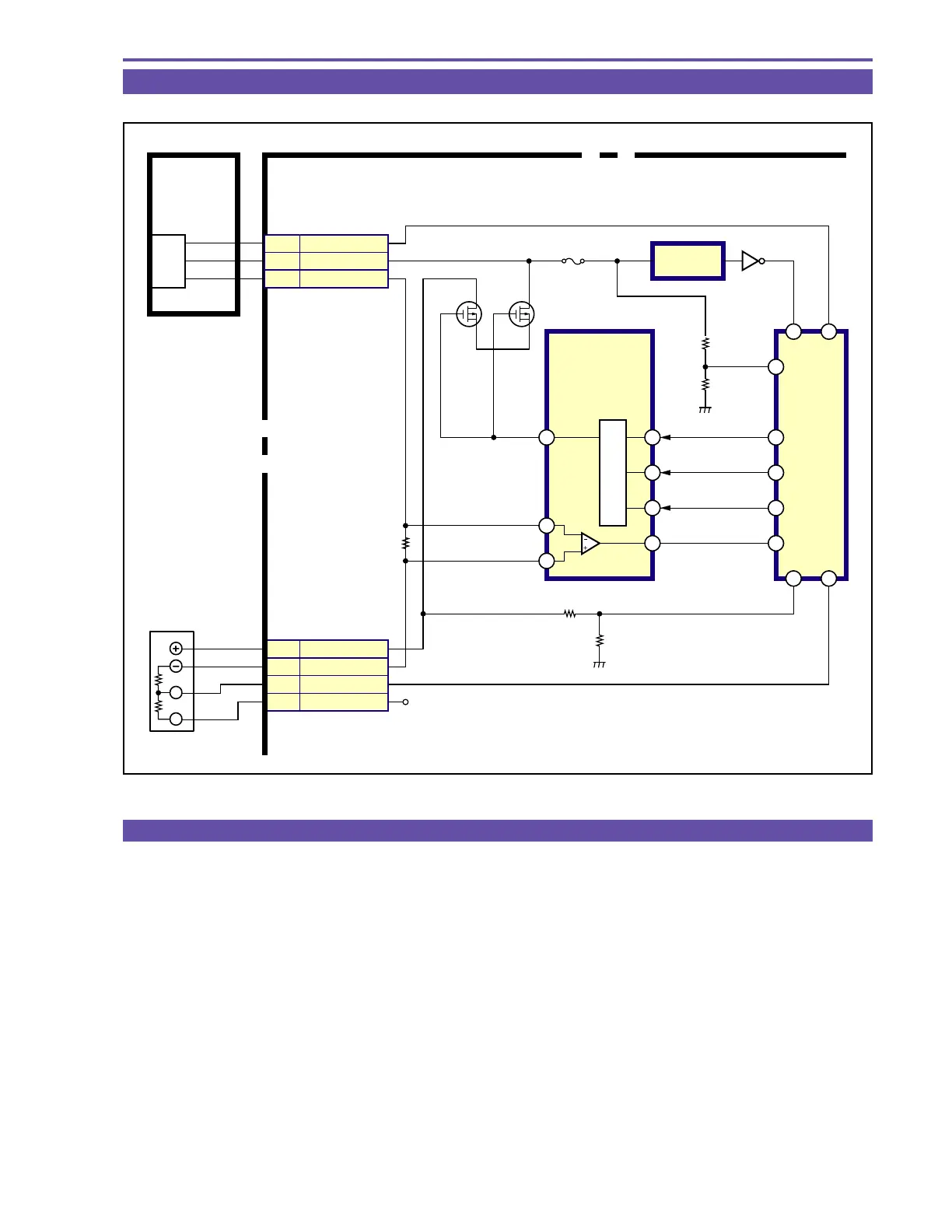
3. Built-in Charger Circuit
3-1 Outline
The main circuit elements and their functions are as follows.
(1) IC100 : MODE MI-COM
• Charging voltage and charging current control
• Detection and display of charging progress
• Error discrimination and display
• Battery type discrimination and DC jack input detection
(2) IC 1800 : Charge control IC
• Signal amplification for detecting charging current
• Charge switch control
• Trickle charge switch / quick charge changeover
(3) Q1800/Q1801 : MOS form FET
• Power supply changeover switch
Fig. 4
CHG-CTL3
CHG-CTL2
A/D I
A/D V
DC JACK DET
UNREG DET
BATT AD
BATT INFO AD
CN3202
5,6
3,4
2
1
BATT+
BATT-
BATT INFO AD
BATT E3
E3
CN3201
DC
JACK
BATTERY
B
D
MAIN P.C.B.
DC
P.C.B.
3
2
1
DC JACK SW
DC+
DC-
8889
7173
90
100
99
CHG-CTL1
Q1801Q1800
41
7
9
6
5
87
IC100
MODE
MI-COM.
IC1800
CHARGE
CONTROL
IC103
RESET
11
10
3
CONTROL