2 Module Description
2.1 Block Diagram
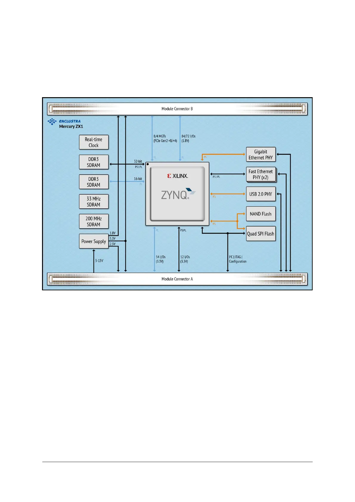
Figure 1: Hardware Block Diagram
The main component of the Mercury ZX1 SoC module is the Xilinx Zynq-7000 SoC device. Most of its I/O
pins are connected to the Mercury module connector, making up to 150 regular user I/Os available to the
user. Further, up to eight multi-gigabit transceivers with support for PCIe Gen2 ×8 are available on the
module connector.
The SoC device can boot from the on-board QSPI flash, NAND flash or from an external SD card. For de-
velopment purposes, a JTAG interface is connected to Mercury module connector.
The memory subsystem is built from a 512 MB NAND flash, a 64 MB quad SPI flash, 1 GB DDR3 SDRAM con-
nected to the Processing System (PS) and 256 MB DDR3 SDRAM connected to the Programmable Logic (PL).
Further, the module is equipped with a Gigabit Ethernet PHY, dual Fast Ethernet PHY, and a USB 2.0 OTG
PHY, making it ideal for communication applications.
A real-time clock is available on the module and is connected to the global I2C bus.
On-board clock generation is based on a 33.33 MHz crystal oscillator for the PS and a 200 MHz LVDS oscil-
lator for the PL.
D-0000-403-002 10 / 56 Version 05, 25.07.2019

 Loading...

