2.18 NAND Flash
The NAND flash can be used to boot the PS, to store the FPGA bitstream, ARM application code and other
user data. Refer to Section 3.3 for details on available boot modes.
The NAND flash is disabled when VCC_CFG_MIO_B12 is 1.8 V. The NAND_ENABLE signal, which controls the
CE# and WP# pins of the NAND flash, is set automatically to GND (if VCC_CFG_MIO_B12 is less than or equal
to 1.8 V) or to VCCO (if VCC_CFG_MIO_B12 is 2.5 V or 3.3 V).
2.18.1 NAND Flash Type
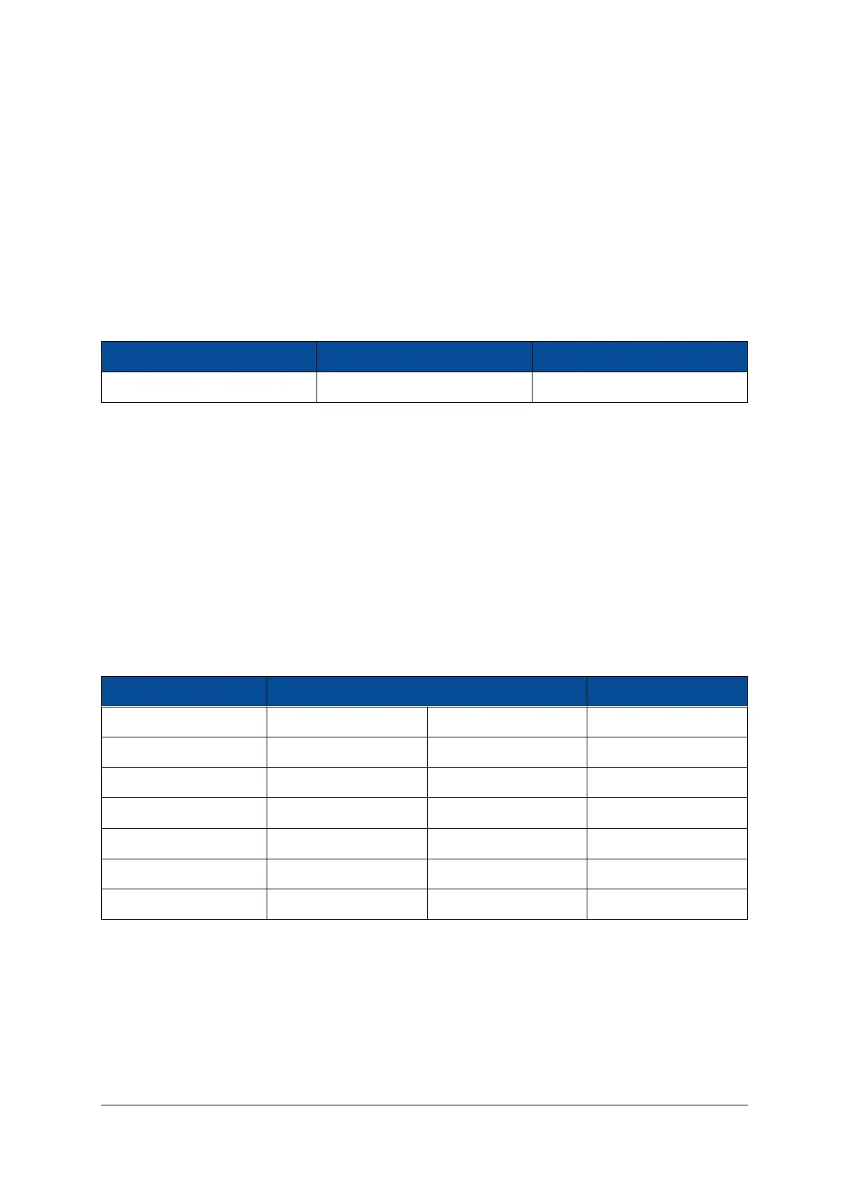
Table 27 describes the memory availability and configuration on the Mercury ZX1 SoC module.
Flash Type Size Manufacturer
MT29F4G08ABADAWP 4 Gbit Micron
Table 27: NAND Flash Type
2.18.2 Signal Description
The NAND flash is connected to the PS MIO pins 0, 2-14. The MIO pins 2-6 are shared between the QSPI
and NAND flash.
2.18.3 Parameters
Please refer to the NAND flash memory device datasheet to extract the required parameter values. Refer-
ence values to be used in Vivado are given in Table 28.
The indicated parameter values may be used for booting from NAND flash memory on the Mercury ZX1
SoC module.
Nand Cycle Parameter CS0 CS0 Cycles Description
T_RC 30 4 Read cycle time
T_WC 30 4 Write cycle time
T_REA 0 1 RE assertion delay
T_WP 20 3 WE deassertion delay
T_CLR 20 3 Page cycle time
T_AR 20 3 ID read time
T_RR 30 4 Busy to RE
Table 28: NAND Flash Parameters
2.19 SD Card
An SD card can be connected to the PS MIO pins 40-45 or 46-51, or alternatively via EMIO pins to the PL.
D-0000-403-002 35 / 56 Version 05, 25.07.2019

 Loading...

