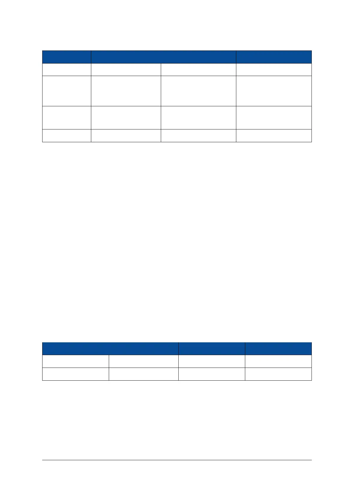
Pin Name Module Connector Pin Connection Description
VMON_1V0 A-102 VCC_INT PS and PL core voltages
VMON_1V2 B-167 VCC_1V2 1.2 V on-board voltage (de-
fault)/SoC battery voltage
(assembly option)
VMON_2V9_DIV B-168 VCC_2V9 on-board voltage
divided by 2
NAND flash supply
VMON_DDR3 B-8 VCC_DDR3 DDR3 voltage
Table 18: Voltage Monitoring Outputs
2.12 Clock Generation
A 33.33 MHz oscillator is used for the Mercury ZX1 SoC module clock generation; the 33.33 MHz clock
(CLK_33) is fed to the PS via PS_CLK pin. This clock is not connected directly to any clock pin of the FPGA
fabric.
A 200 MHz LVDS oscillator is connected to FPGA bank 33 (pins L4 and L5). The signal is terminated with a
100 Ω parallel resistor close to the FPGA pins.
2.13 Reset
The power-on reset signal (POR) and the PS system reset signal (SRST) of the SoC device are available on
the module connector.
Pulling PS_POR# low resets the SoC device, the Ethernet and the USB PHYs, and the flash devices. Please
refer to the Enclustra Module Pin Connection Guidelines [10] for general rules regarding the connection of
reset pins.
Pulling PS_SRST# low resets the SoC device. For details on the functions of the PS_POR_B and PS_SRST_B
signals refer to the Zynq-7000 Technical Reference Manual [18].
Table 19 presents the available reset signals. Both signals, PS_POR# and PS_SRST#, have on-board 10 kΩ
pull-up resistors to VCC_CFG_MIO_B12.
Signal Name Module Connector Pin FPGA Pin Type Description
PS_POR# A-132 PS_POR_B Power-on reset
PS_SRST# A-124 PS_SRST_B System reset
Table 19: Reset Resources
Please note that PS_POR# is automatically asserted if PWR_GOOD is low.
2.14 LEDs
There are four active-low LEDs on the Mercury ZX1 SoC module. LEDs 0-2 are connected to the FPGA logic
and LED3 is connected to the pin MIO15 of the PS.
D-0000-403-002 28 / 56 Version 05, 25.07.2019

 Loading...

