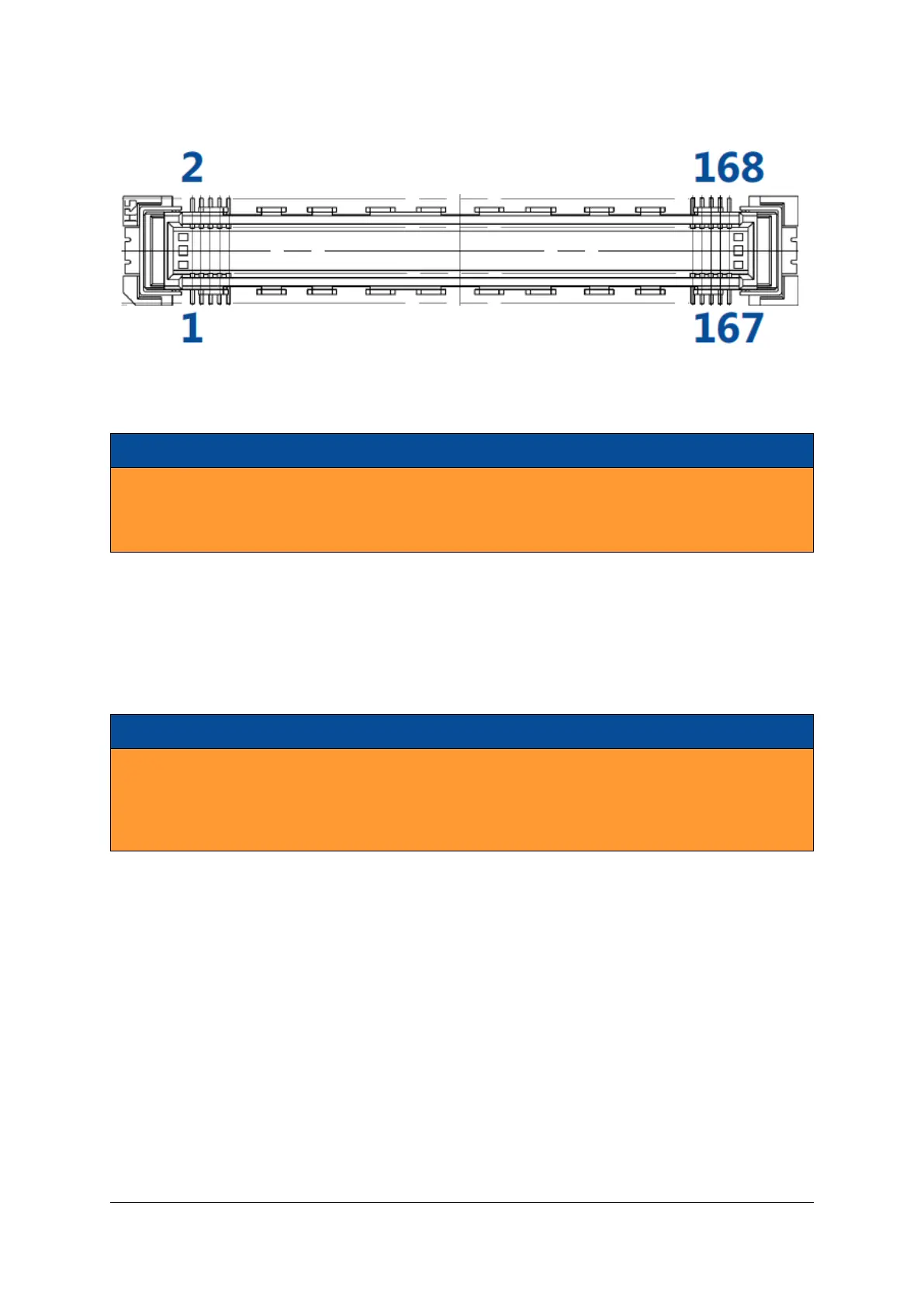
Figure 9: Pin Numbering for the Module Connector
Warning!
Do not use excessive force to latch a Mercury module into the Mercury connectors on the base board,
as this could damage the module and the base board; always make sure that the module is correctly
oriented before mounting it into the base board.
2.9 User I/O
2.9.1 Pinout
Information on the Mercury ZX1 SoC module pinout can be found in the Enclustra Mercury Master Pinout
[11], and in the additional document Enclustra Module Pin Connection Guidelines [10].
Warning!
Please note that the pin types on the schematics symbol of the module connector and in the Master
Pinout document are for reference only. On the Mercury ZX1 SoC module it may be possible that
the connected pins do not have the targeted functions (such as primary clocks, differential pins, MGT
signals, etc).
The naming convention for the user I/Os is:
IO_B<BANK>_L<PAIR><_SPECIAL_FUNCTION>_<PACKAGE_PIN>_<POLARITY>.
For example, IO_B33_L12_MRCC_J3_N is located on pin J3 of I/O bank 33, pair 12, it is an MRCC (Multi-Region
Clock Capable) pin and it has negative polarity, when used in a differential pair.
For the signal lines shared between Programmable Logic (PL) and Processing System (PS), the naming con-
vention is:
IO_<MIO_PIN>_<FUNCTION>_B<BANK>_<PACKAGE_PIN>
For example, IO_MIO44_SDD2_B12_AC17 is connected to FPGA pin AC17 and in parallel to the PS MIO pin 44.
Please note that for the shared pins only one of the driving pins (FPGA pin, MIO pin) may be active.
The multi-region clock capable pins are marked with “MRCC”, while the single region clock capable pins are
marked with “SRCC” in the signal name. For details on their function and usage, please refer to the Xilinx
D-0000-403-002 17 / 56 Version 05, 25.07.2019

 Loading...

