documentation.
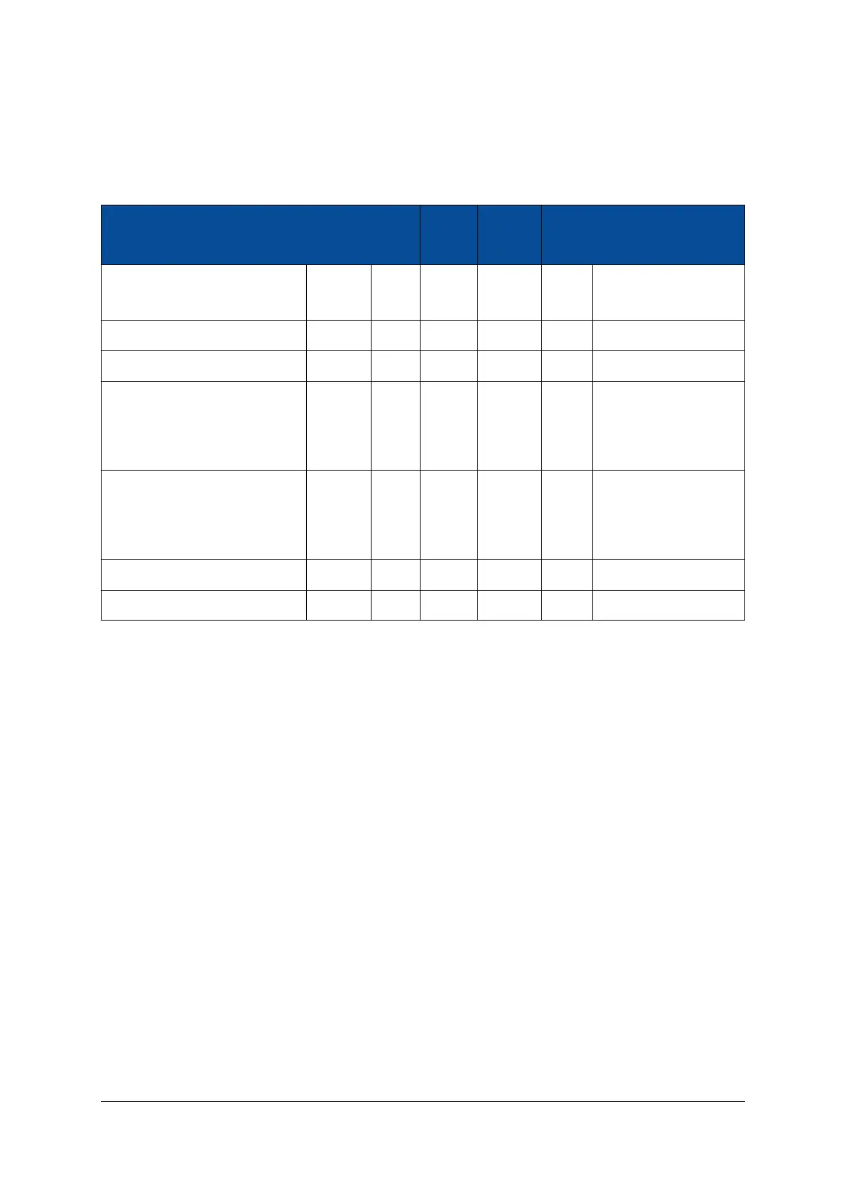
Table 6 includes information related to the total number of I/Os available in each I/O bank and possible
limitations.
Signal Name Signals Pairs Diff. Single- I/O Comments
ended Bank
IO_<MIO_PIN>_<...>_B12_<...> 12 6 In/Out In/Out 12 Shared between PL
and PS
IO_B12_<...> 4 2 In/Out In/Out 12
IO_B13_<...> 50 24 In/Out In/Out 13
IO_B33_<...> 46 23 In/Out In/Out 33 Only 36 sig-
nals available on
XC7Z035/XC7Z045
devices
IO_B34_<...> 38 19 In/Out In/Out 34 Only 36 sig-
nals available on
XC7Z035/XC7Z045
devices
Total (XC7Z030) 150 75 - - -
Total (XC7Z035/XC7Z045) 138 68 - - -
Table 6: User I/Os
Please note that for the 7 Series FPGAs there are restrictions on the VCCO voltage when using LVDS I/Os;
refer to Xilinx AR# 43989 for details.
2.9.2 I/O Pin Exceptions
The I/O pin exceptions are pins with special functions or restrictions.
I/O Pins with Different Functions Depending on the Equipped SoC Device
On the Mercury ZX1 SoC modules equipped with bigger SoC devices (XC7Z035/XC7Z045) there are eight
MGT transceiver lines and four differential clock inputs available.
On the modules equipped with smaller SoC devices (XC7Z030) there are only four MGT transceiver lines and
2 differential clock inputs available. Instead, the transmission (TX) signals of the upper MGT pairs (pairs 4-7)
and two differential clock pairs are rerouted to regular user I/Os from FPGA banks 33 and 34. The receiver
(RX) signals of the upper MGT pairs are not connected to any FPGA bank on the smaller module.
Table 7 presents the I/O pin exceptions on the Mercury ZX1 SoC module.
D-0000-403-002 18 / 56 Version 05, 25.07.2019

 Loading...

