I/O Module Description
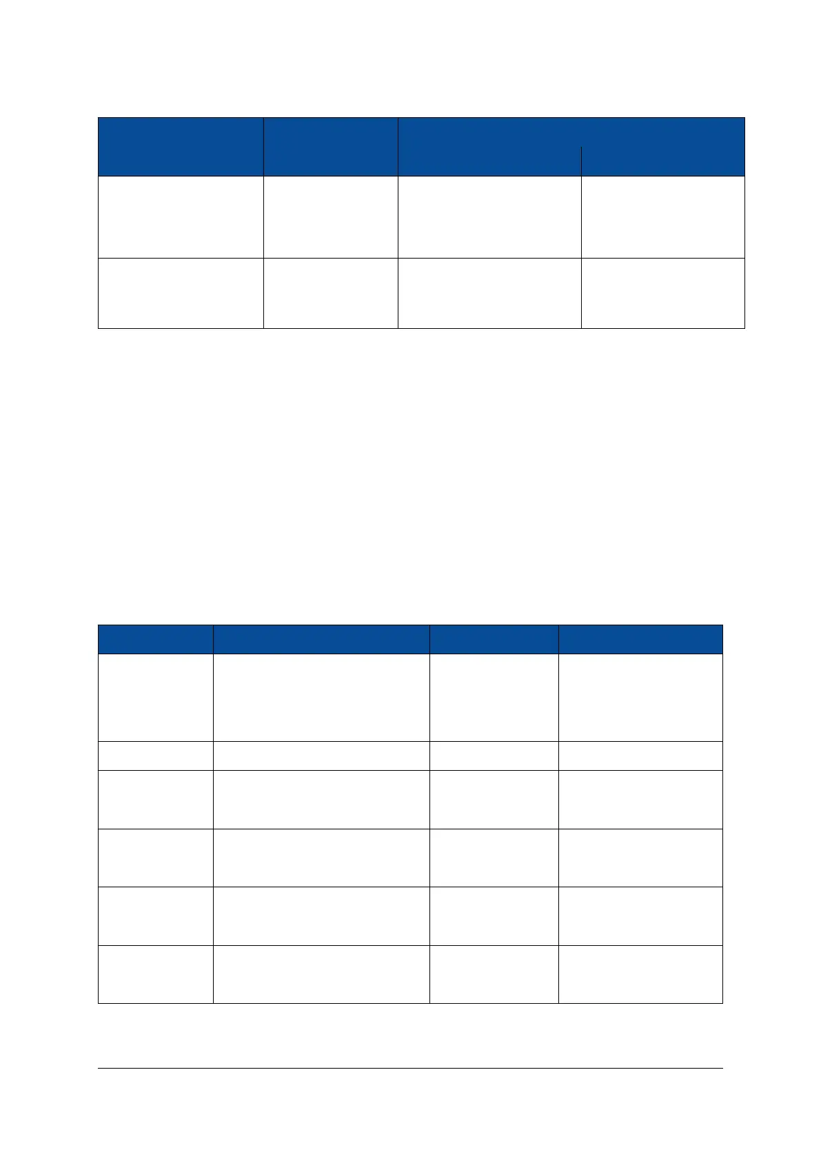
Name Conn. Pin XC7Z030 XC7Z035/XC7Z045
MGT_REFCLK<2-3>_<...> B-3, 5, 7, 9
These pins are connected to
user I/Os in FPGA banks 33
and 34
These pins are connected
to the MGTs in FPGA
bank 111
MGT_TX<4-7>_<...> B-45, 47, 51, 53, 63,
65, 69, 71
MGT_RX<4-7>_<...> B-48, 50, 54, 56, 60,
62, 66, 68
These pins are not con-
nected
These pins are connected
to the MGTs in FPGA
bank 111
Table 7: I/O Pin Exceptions - I/O Pins with Different Functions Depending on the Equipped SoC Device
2.9.3 Differential I/Os
When using differential pairs, a differential impedance of 100 Ω must be matched on the base board, and
the two nets of a differential pair must have the same length.
The information regarding the length of the signal lines from the SoC device to the module connector is
available in Mercury ZX1 SoC Module IO Net Length Excel Sheet [3]. This enables the user to match the total
length of the differential pairs on the base board if required by the application.
2.9.4 I/O Banks
Table 8 describes the main attributes of the Programmable Logic (PL) and Processing System (PS) I/O banks,
and indicates which peripherals are connected to each I/O bank. All I/O pins within a particular I/O bank
must use the same I/O (VCC_IO) and reference (VREF) voltages.
Bank Connectivity VCC_IO VREF
MGT Bank 111
Module connector 1.2 V -
(not available on
XC7Z030 device)
MGT Bank 112 Module connector 1.2 V -
Bank 0 Configuration
User selectable
-
VCC_CFG_MIO_B12
Bank 12
Module connector, User selectable -
Fast Ethernet PHYs, I2C VCC_CFG_MIO_B12
Bank 13 Module connector
User selectable IO_B13_L6_VREF_AB24_N
VCC_IO_B13 IO_B13_L19_VREF_Y20_N
Bank 33 Module connector, oscillator
User selectable IO_B33_L6_VREF_E3_N
VCC_IO_B33 IO_B33_L19_VREF_L7_N
Continued on next page...
D-0000-403-002 19 / 56 Version 05, 25.07.2019

 Loading...

