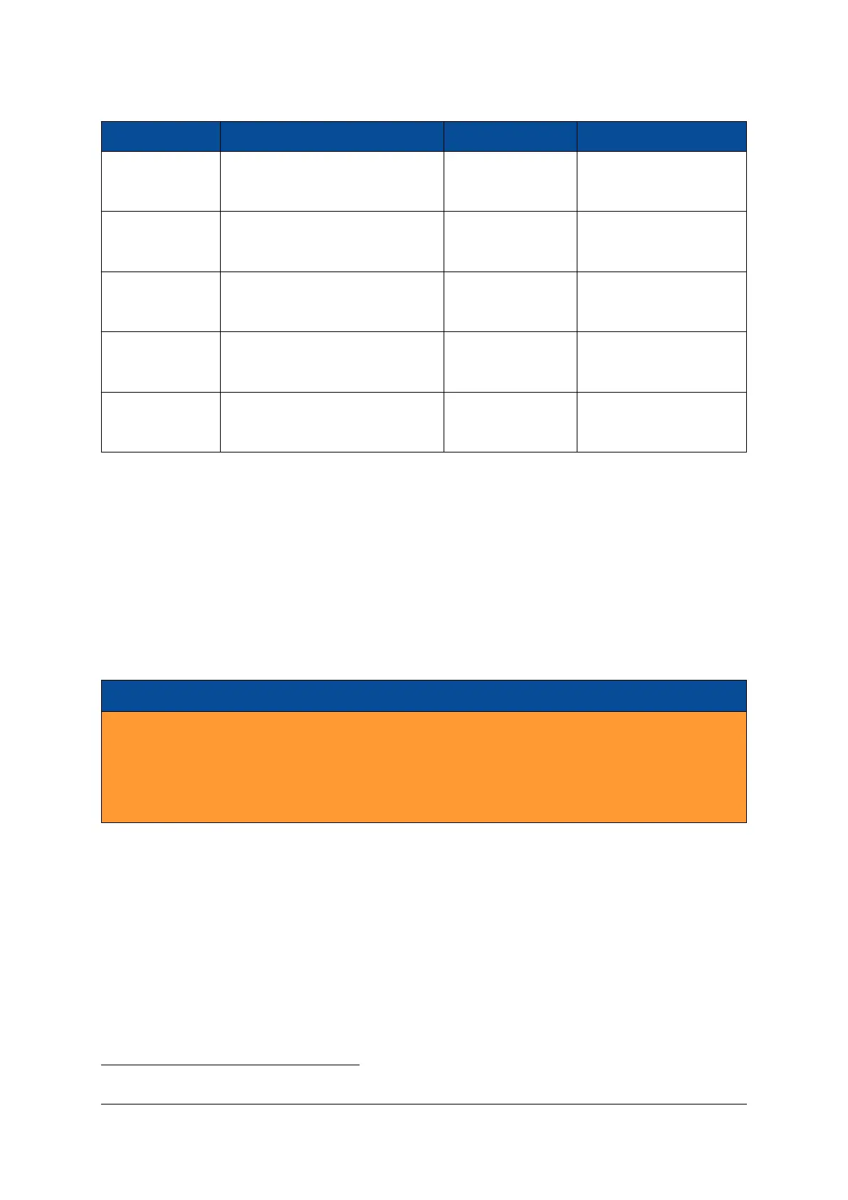
Bank Connectivity VCC_IO VREF
Bank 34
Module connector, I2C, User selectable IO_B34_L6_VREF_H8_N
Fast Ethernet PHYs, LEDs VCC_IO_B34 IO_B34_L19_VREF_C3_N
Bank 35 DDR3 SDRAM (PL)
User selectable
1
0.5 × VCC_DDR3
VCC_DDR3
PS MIO0 QSPI and NAND flash
User selectable
-
VCC_CFG_MIO_B12
PS MIO1
Module connector, USB PHY, User selectable
0.9 V
Gigabit Ethernet PHY VCC_CFG_MIO_B12
PS DDR DDR3 SDRAM (PS)
User selectable
1
0.5 × VCC_DDR3
VCC_DDR3
Table 8: I/O Banks
1
2.9.5 VREF Usage
I/O standards referenced using VREF can be used on the Mercury module connector. The reference voltage
has to be applied to all VREF pins of the respective I/O banks. If a bank is configured to use an I/O standard
that does not need a reference voltage, the VREF pins of this bank on the module connector are available
as user I/O pins.
The VREF pins are listed in the Mercury Master Pinout Excel Sheet [11].
Warning!
Use only VREF voltages compliant with the equipped SoC device; any other voltages may damage the
equipped SoC device, as well as other devices on the Mercury ZX1 SoC module.
Do not leave a VREF pin floating when the used I/O standard requires a reference voltage, as this may
damage the equipped SoC device, as well as other devices on the Mercury ZX1 SoC module.
2.9.6 VCC_IO Usage
The VCC_IO voltages for the I/O banks located on the module connector are configurable by applying the
required voltage to the VCC_IO_B[x], respectively VCC_CFG_[x] pins. All VCC_IO_B[x] or VCC_CFG_[x] pins of
the same bank must be connected to the same voltage.
For compatibility with other Enclustra Mercury modules, it is recommended to use a single I/O voltage per
module connector.
The high performance (HP) I/O banks 33 and 34 are protected against too high supply voltages. If a voltage
higher than 2.2 V is applied to the corresponding supply inputs on the module connector, the supply pins
of the SoC device are disconnected, and the device is held in reset.
1
The DDR3 SDRAM supports voltages of 1.5 or 1.35 V. Please refer to Sections 2.15 and 2.16 for details.
D-0000-403-002 20 / 56 Version 05, 25.07.2019

 Loading...

