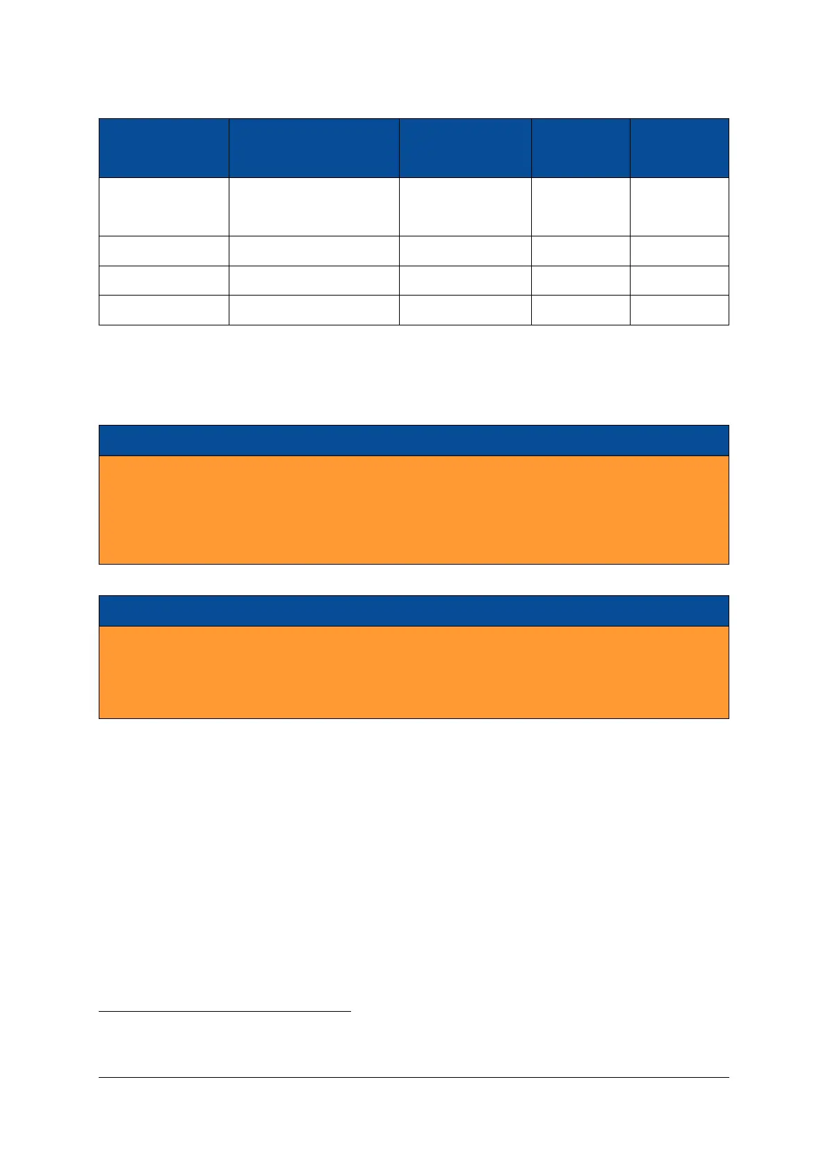
Signal Name SoC Pins Supported Connector Connector
Voltages A Pins B Pins
VCC_CFG_MIO_B12
VCCO_0, VCC_IO_B12, 1.8 V
2
,
74, 77 -
VCCO_MIO0, VCCO_MIO1 2.5 V - 3.3 V
3
±5%
VCC_IO_B13 VCCO_13 1.2 V - 3.3 V ±5% 38, 41 -
VCC_IO_B33 VCCO_33 1.35 V - 1.8 V ±5% - 67, 95, 143
VCC_IO_B34 VCCO_34 1.35 V
4
- 1.8 V ±5% - 64, 88, 140
Table 9: VCC_IO Pins
2 3 4
Note that the CFGBVS_0 pin is set automatically to GND (if VCC_CFG_MIO_B12 is less than or equal to 1.8 V)
or to VCCO (if VCC_CFG_MIO_B12 is 2.5 V or 3.3 V).
Warning!
Use only VCC_IO voltages compliant with the equipped SoC device; any other voltages may damage
the equipped SoC device, as well as other devices on the Mercury ZX1 SoC module.
Do not leave a VCC_IO pin floating, as this may damage the equipped SoC device, as well as other
devices on the Mercury ZX1 SoC module.
Warning!
Do not power the VCC_IO pins when PWR_GOOD and PWR_EN signals are not active. If the module
is not powered, you need to make sure that the VCC_IO voltages are disabled (for example, by using a
switch on the base board, which uses PWR_GOOD as enable signal). Figure 10 illustrates the VCC_IO
power requirements.
2
NAND flash is disabled when VCC_CFG_MIO_B12 is 1.8 V.
3
The RGMII Ethernet interface is specified only up to 2.5 V on the MIO pins by Xilinx. Please refer to Section 2.20 for details.
4
The LEDs may start to glow when VCC_IO_B34 is less than 1.8 V.
D-0000-403-002 21 / 56 Version 05, 25.07.2019

 Loading...

