REV.-A
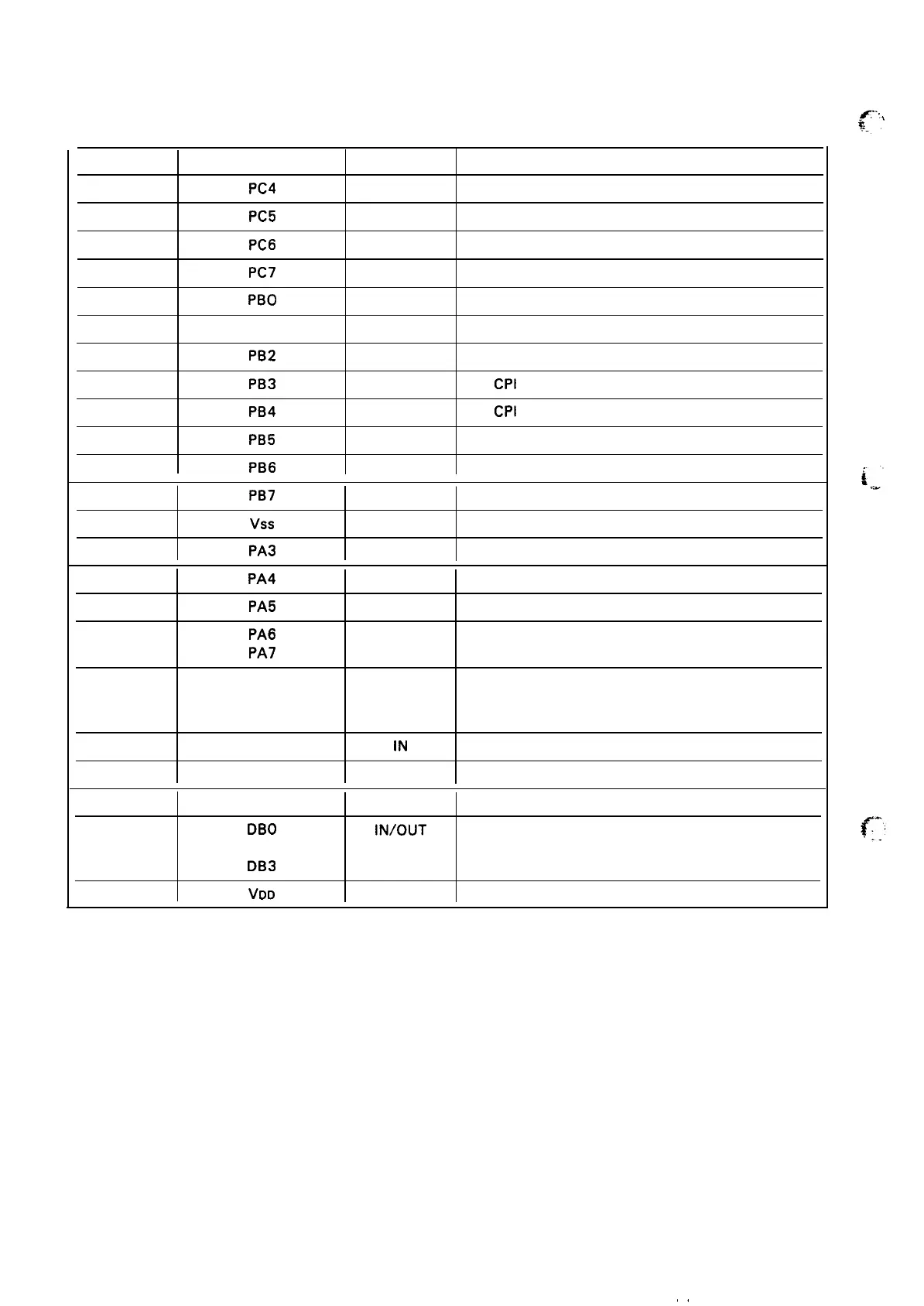
Table 2-5. Pin Function of GA (E05A16GA) (cent’d)
Pin No.
Signal Name
Direction
Function
36
PC4
OUT
PAPER OUT LED ON/OFF Control Signal
37
PC5
OUT
READY LED ON\ OFF control signal
38
PC6
OUT
ON LINE LED ON/OFF control signal
39
PC7
—
Not used
40
PBO
OUT
DRAFT LED ON/OFF control signal
41
PB 1
OUT
ROMAN LED ON/OFF control signal
42
PB2
OUT
SANS SERIF LED ON/OFF control signal
43
PB3
OUT
10
CPI
(PICA) LED ON/OFF control signal
44
PB4
OUT
12
CPI
(ELITE) LED ON/OFF control signal
45
PB5
OUT
PS (PROPORTIONAL) LED ON/OFF control signal
46
PB6
OUT
CONDENSED LED ON/OFF control signal
47
PB7
—
Not used
48
Vss
—
Logic ground
49
PA3
IN
LINE FEED switch
50
PA4
IN
FORM FEED switch
51 PA5
IN
LOAD/EJECT switch
52
PA6
—
Not used
53
PA7
54
AO IN
Address bit (AO - A2)
I
I
56
A2
57 Cs
IN
Chip Select signal input
58
RD
IN
Read strobe signal
59 WR
IN
Write strobe signal
55
DBO
lN\OUT
Input/Output data bus (DO - D3)
I
I
63
DB3
64
Vrm
IN
Power source
NOTE: “Direction” on the signal flow is as viewed from the gate array.
2-32
 Loading...