GE Power Management
ALPS Advanced Line Protection System 3-7
3 HARDWARE DESCRIPTION 3.3 PRINTED CIRCUIT BOARD MODULES
3
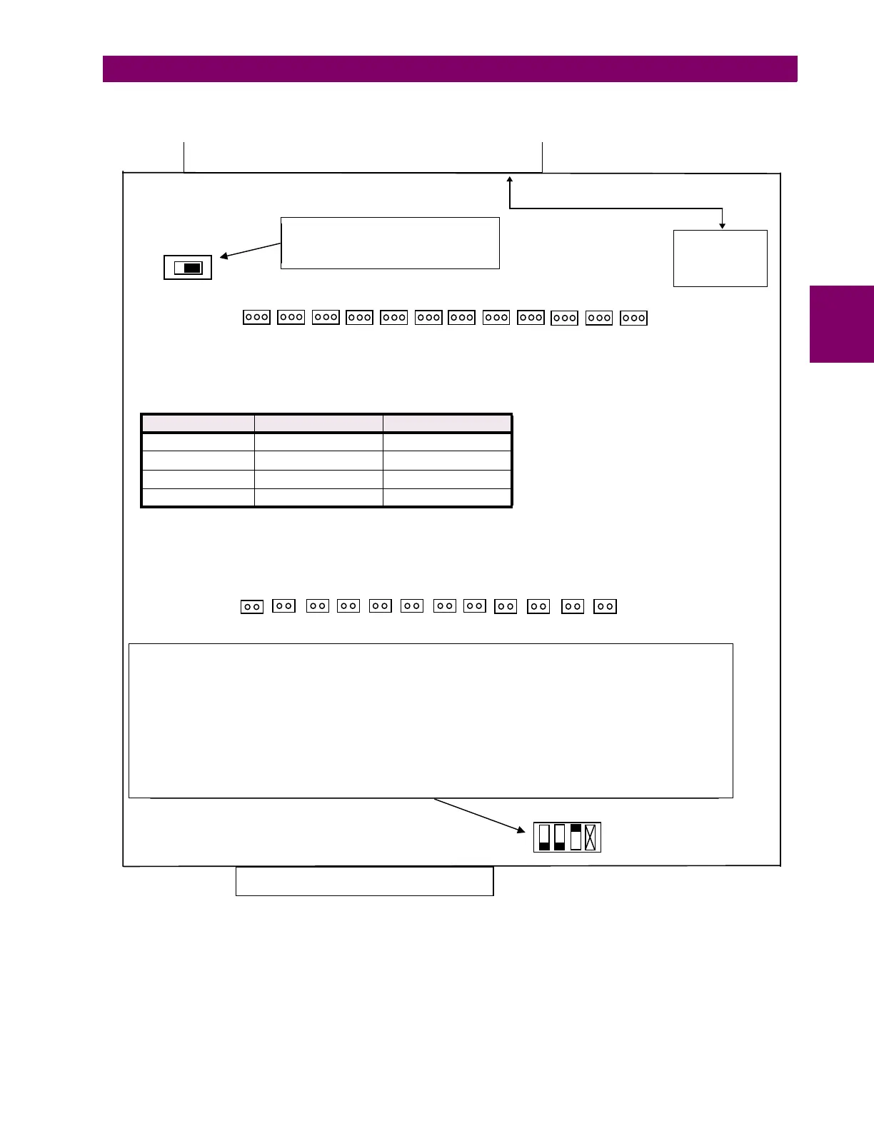
Figure 3–5: INPUT BOARD DIAGRAM
SW1 determines I or V for the SCADA
I/F. Left switch position is volta
e
Ri
ht Switch Position is current
IRIG-B REAL
TIME CLOCK
INPUT
EDGE CONNECTOR
J12 J11 J10 J9 J8 J7 J6 J5 J4 J3 J2 J1
VI
SW1
J1 throu
h J24 select the input DC volta
e ran
e for the di
ital input contact converters. Refer to the table below for jumper
placement. Place jumper on 1 pin for OPEN position, otherwise place jumper as desi
nated
† Some Input boards only have J1-J12 and are dual ran
e inputs only. Jumper in = 38.5 to 300V; Jumper out = 80 to 300V.
Table 3–1: JUMPER POSITION
INPUT RANGE † J1-J12 POSITION J13-J14 POSITION
5V - 300V DC 1-2 IN
8V - 300V DC 1-2 OPEN
38.5V - 300V DC 2-3 OPEN
80V - 300V DC OPEN OPEN
J24 J23 J22 J21 J20 J19 J18 J17 J16 J15 J14 J13
Switch 1: KEYBOARD EN ON (Keyboard Enable) - UP keypad is disabled / DOWN keypad is enabled †
Switch 2: RM SETT CHG ON (Remote Settin
s Chan
e) - UP settin
s chan
es throu
h communications is dis-
abled / DOWN enabled †
Switch 3: RM BRKR ON (Remote Breaker Operation) - UP breaker operations throu
h communications disabled
† / DOWN enabled
Switch 4: Not used
NOTE: Relay Power switch must be in the off position before chan
in
switch positions
† Default position
BUS CARD CONNECTOR
OPTION
SWITCH
12 34