2JN
2-3-10
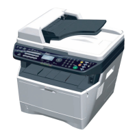
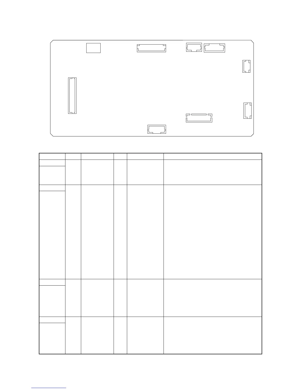
Figure 2-3-6Scanner PWB silk-screen diagram
Connector Pin Signal I/O Voltage Description
YC101 1 +24V1 O 24 V DC 24 V DC power source
Connected
to the power
source PWB
2 N.C. - - Not used
3 GND - - Ground
YC102 1 SEGIR O 0/3.3 V DC Serial communications interruption demand
Connected
to the con-
trol PWB
2 SSDIR O 0/3.3 V DC Serial communications trans./recep. change
3 SSBSY O 0/3.3 V DC Impossible transmission/Completion notice
4 SEGSI I 0/3.3 V DC (pulse) Serial communications data output
5 SSCKN I 0/3.3 V DC (pulse) Serial communications clock
6 SEGSO O 0/3.3 V DC Vertical synchronizing signal
7 PAGESET I 0/3.3 V DC Vertical synchronizing monitor signal
8 OVMONOUT I 0/3.3 V DC Communications ready signal
9 CPURDY I 0/3.3 V DC Communications ready signal
10 CPUSEL O 0/3.3 V DC Communications select signal
11 CPUSO I 0/3.3 V DC (pulse)
Serial communications data input
12 CPUSI O 0/3.3 V DC (pulse) Serial communications data output
13 CPUCLK O 0/3.3 V DC (pulse) Serial communications clock signal
14 +3.3V1 I 3.3 V DC 3.3 V DC power source
15 GND - - Ground
YC103 1 +12V I 12 V DC 12 V DC power source
Connected
to the con-
trol PWB
2 GND - - Ground
3 HPSW I 0/3.3 V DC Home position sensor: On/Off
4 GND - - Ground
5 NC - - Not used
6 LAMP I 0/24 V DC Exposure lamp drive signal
YC104 1 SCMOT1A O 0/24 V DC (pulse) ISU motor drive pulse
Connected
to the ISU
motor
2 SCMOT2B O 0/24 V DC (pulse) ISU motor drive pulse
3 SCMOT1B O 0/24 V DC (pulse) ISU motor drive pulse
4 SCMOT2A O 0/24 V DC (pulse) ISU motor drive pulse
YC101
YC109
YC108YC104
YC106
YC107
YC105
YC103
YC102
1
1
1
1
1
15
9
10
1
2
7
1
5
6
14
15
2
1
2
4
6
2
3
 Loading...