NSW-5
Disassembly and Troubleshooting Instructions
PAMS Technical Documentation
Page 21
Issue 1 10/00
Nokia Mobile Phones Ltd.
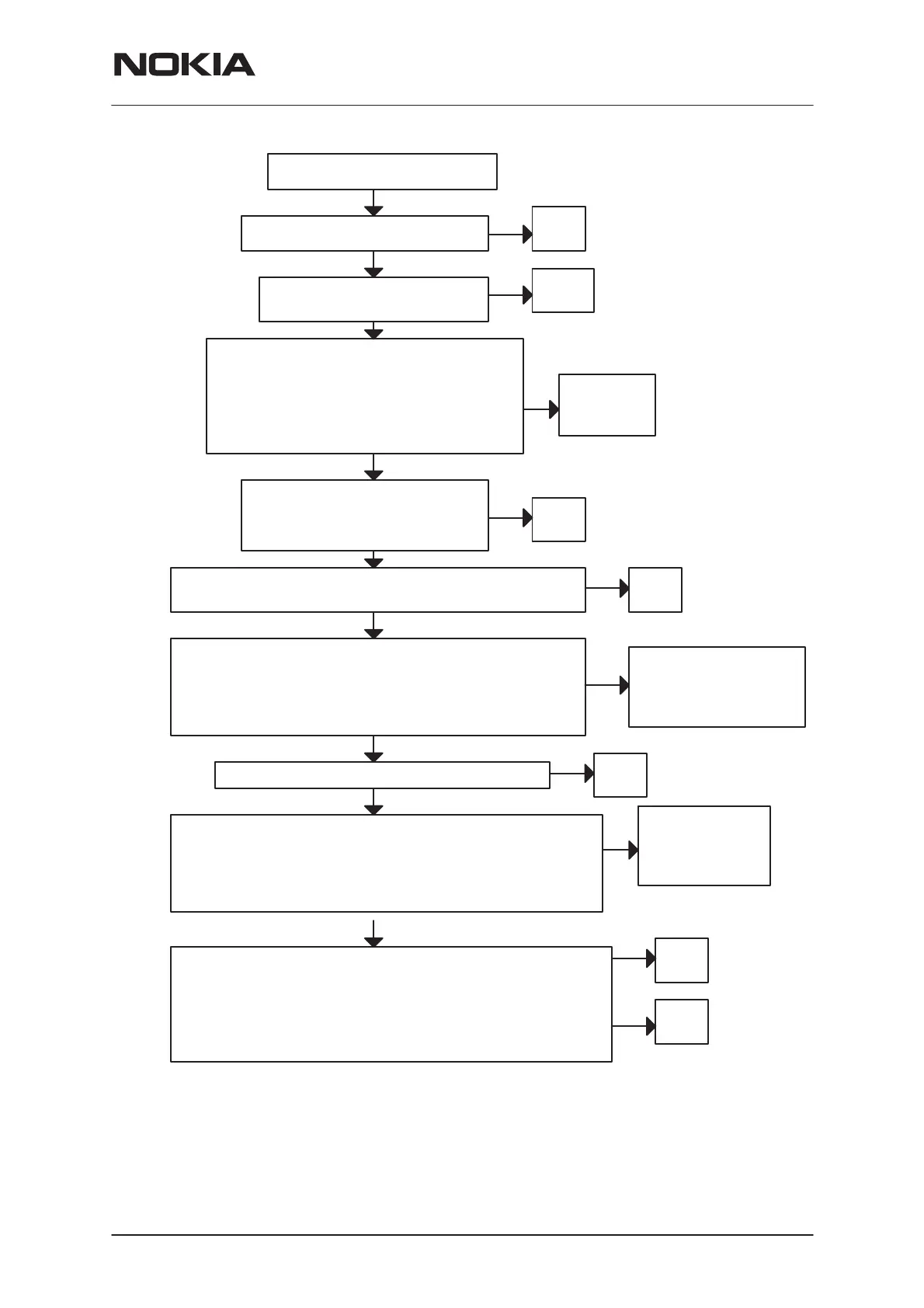
Phone doesn’t register to the network
or phone doesn’t make a call
YES
Analog supply voltage VR6 is > 2.7 V of
Cobba (N250) at C275
NO
YES
Check
N250
Analog reference voltage Vref is 1.5 V
of Cobba (N250) at C169
NO Check
R256
YES
YES
NO
Synthesizer lines: SENA2 (N880 pin 13 ),
SCLK (N880 pin 11)
SDATA (N880 pin 12)
pulses 0 –> 1 during off burst
NO
YES
AFC (R850) 0 –> 1.2 V typ. during receiving burst
NO
YES
Analog data signal IF2AN (R789) –> 0.2 Vpp, 0–>2.2 V DC
Analog data signal IF2AP (R788) –> 0.2 Vpp, 0–>2.2 V DC
NO
Check
COBBA N250 if DC fails
Check
RF part if AC signal fails
YES
DAX signal (J208) pulses 1 –> 0 during receiving slot
NO
Check
N250
TX control lines:
TXC (N750 pin 1, R752) 0 –> 2.3 Vmax during transmit burst
TXA (N750 pin 2, R751) goes 0–>1 (2.8 V) during modulation
YES
Check
N250 if TxC is failed
Check
D202 if TXA is failed
NO
YES
Analog data signals: TxIN (N750 pin 10) 0–> 0.8 V DC during transmit slot
TxIP (N750 pin 9) 0 –> 0.8 V DC during transmit slot
TxQN (N750 pin 7) 0 –> 0.8 V DC during transmit slot
TxQP (N750 pin 8) 0 –>0.8 V DC during transmit slot
Used IQ signals are biased to 0.8V DC and AC amplitude is 400 mVpp
max, frequency is 12 kHz max
NO
Check
N250
YES
Check
RF part
MAD D202
CCONT N150
MAD
COBBA
D202
N250
TXLX are low during PL7 to PL2 and high during PL10 to PL 8
AGC1 (R758) 0 –> 2.3 V max during receiving burst
Digital data signal IF2DN (C750) –>170 mVpp typ,
Digital data signal IF2DP (C751) –>170 mVpp typ, 0–> 2.7 V DC
Frequency is 450 MHz
0–> 2.7 V DC
TXLX1 (R934 pin 1) and TXLX2 (R934 pin 2) 0–> 1 (2.8 V)
Check supply voltages for RF:
Check
COBBA
MAD
RX: VR1 (C158), VR2 (C159), VR3 (C160), VR4 (C161),
VR5 (C162), VR8 (N702 pin 14), VR9 (N702 pin 13),
VR10 (N702 pin 12) and V5V (C176)
TX: VR3 (C160), VR7 (C164), VR7_bias (R901),
VR11 (N702 pin 11), VR12 (N702 pin 9) and
TXPWR3 (C903)
 Loading...