NSW-5
Disassembly and Troubleshooting Instructions
PAMS Technical Documentation
Page 54
Issue 1 10/00
Nokia Mobile Phones Ltd.
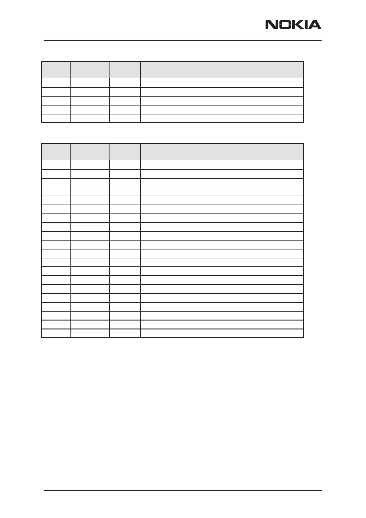
DescriptionNominal
level
Pin namePin no.
12 VDD3 2.8V Supply voltage
13 GND 0 Ground
14 IF IN – Intermediate frequency input
15 N/C Not connected
16 TX ENA >2V TX enable
TDMA 1900 PLL N880
Pin no. Pin name Nominal
level
Description
1 FAST 2.8V Enable input for fast chargepump
2 CPF Fast charge pump output
3 CP Normal charge pump output
4 VDD2 2.8V Power supply voltage
5 Vss3 0 Ground
6 RFI ? Main divider input
7 Vss2 0 Ground
8 POL 2.8V polarity select
9 PON 2.8V Power on input
10 Vss1 0 Ground
11 CLK ? Programming bus clock input
12 DATA ? Programming bus data input
13 E ? Programming bus enable input
14 Vdd1 – Power supply voltage
15 XTALB – Complementary crystal frequency input
16 XTALA – Complementary crystal frequency input
17 GND(CP) 0 Ground for charge pump
18 Vcc 4.8V Supply voltage for charge pump
19 Iset – charge pump currents setting
20 LOCK – Out of lock detector
 Loading...