NSW-5
Disassembly and Troubleshooting Instructions
PAMS Technical Documentation
Page 33
Issue 1 10/00
Nokia Mobile Phones Ltd.
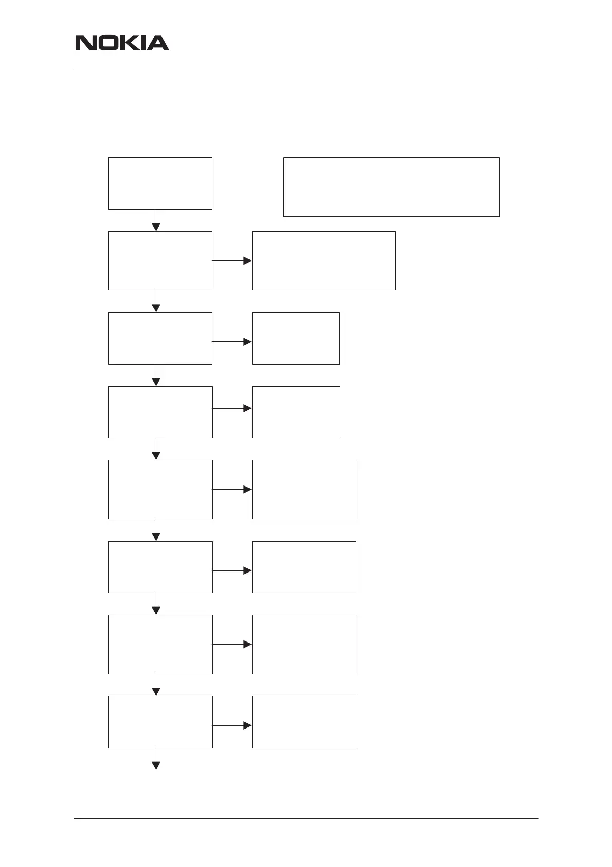
TDMA 800 RX
Apply 879.00 MHz
(Ch 300)–60 dBm
signal (no modulation)
to external antenna
connector (X991)
Check level of
IF2–sinal (450 kHz)
in RF/BB–interface
from resistor R798
P:
≅
–13 dBm
Check UHF VCO
control voltage from
capasitor C831
V: 1.0...4.0 V
Start synthesizer
troubleshooting
Y
N
N
Y
NOTE!
If AMPS RX check is OK, then only
components in
AGC1, OUT_rx, IN(N/P)_rxif
and
OUT(N/P)_rxif
–lines (EROTUS) needs to
be checked.
TDMA 800
RX–chain is OK.
Start baseband troubleshooting
(signal go next to COBBA IC N250)
C
heck 3 multiplier output
level (58.32 MHz)
from coil L762
P:
≅
–10
…–20 dBm
N
N
Check level
(879.00 MHz)
from duplex filter
(Z910) input
P:
≅
–60 dBm
Check level
from frontend (N701)
LNA input pin no.7
P:
≅
–60 dBm
Check level
from LNA output
(N701) pin no.10
P:
≅
–40 dBm
N
Change diplexer Z970
Note!
Check all soldering and
components in antenna
circuit before changing
N
Y
Y
Change duplex filter Z910
or coil L701
Note!
Check all soldering and
discrete components of
frontend.
Change frontend N701
Y
Note!
AGC2 is on
= gain is in high state
(~ 2.8 V at N701 pin no.9)
Check level from MXR
input (N701) pin no.12
P:
≅
0–2 dB less than at LNA
output pin no. 10
Change RX bandfilter Z701
Note!
Check all soldering
N
Y
N
Y
Start synthesizer
troubleshooting
Note!
Signal level!
 Loading...