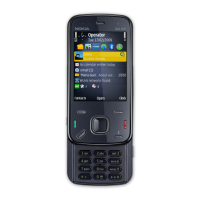
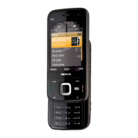
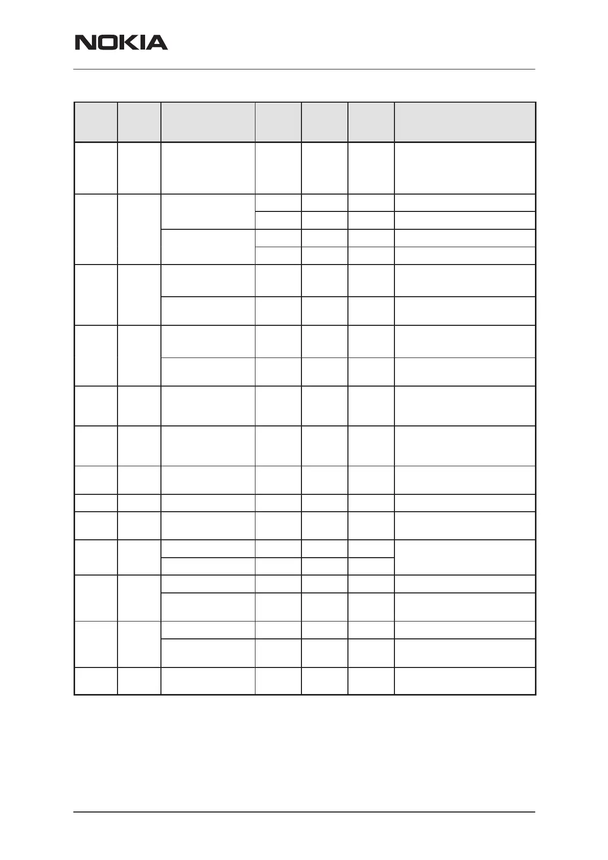
NSW-5
System Module UT5U
PAMS Technical Documentation
Page 9
Issue 1 10/00
Nokia Mobile Phones Ltd.
Unit / NotesMaxi-
mum
Typical
/ Nomi-
nal
Mini-
mum
ParameterLine
Sym-
bol
Con-
tact
pin
CHAR-
GER
JACK
(2)
L_GND Charger ground
input
0 0 0 V/ Supply ground
CHAR-
VIN Charger input
7.1 8.4 9.3 V/ Unloaded ACP-8 Charger
ER
A
K
voltage
720 800 850 mA/ Supply current
(3)
Charger input
7.24 7.6 7.95 V/ Unloaded ACP–7 Charger
current
320 370 420 mA/ Supply current
CHAR-
GER
CHRG
CTRL
Output
high voltage
2.0 2.8 V/ Charger control (PWM)
high
(4)
PWM frequency 32 Hz /PWM frequency for
charger
5 CHRG
CTRL
Output
high voltage
2.0 2.8 V/ Charger control (PWM)
high
PWM frequency 32 Hz /PWM frequency for
charger
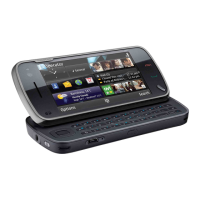
Slide
switch
(6)
SLIDE SLIDE OPEN/
CLOSE
2.7 2.8 2.85 V/ Contact in microphone
cavity.
Slide
switch
(7)
L_GND SLIDE SWITCH
GND
0 0 0 V/ Contact in microphone
cavity.
8 XMIC Input
signal voltage
60 1 Vpp mVrms
9 SGND Signal ground 0 0 mVrms
10 XEAR Output
signal voltage
80 1 Vpp mVrms
11 MBUS
I/O low voltage 0 0.8
V/Serial bidirectional control
I/O high voltage 2.0 2.8
bus. Baud rate 9600 Bit
s
12 FBUS_
Input low voltage 0 0.8 V/ Fbus receive.
RX
Input high voltage 2.0 2.8 V/ Serial Data, Baud rate
9.6k–230.4kBit/s
13 FBUS_
Output low voltage 0 0.8 V/ Fbus transmit.
TX
Output
high voltage
2.0 2.8 V/ Serial Data, Baud rate
9.6k–230.4kBit/s
14 L_GND Common ground
input
0 0 0 V/ Supply ground
 Loading...