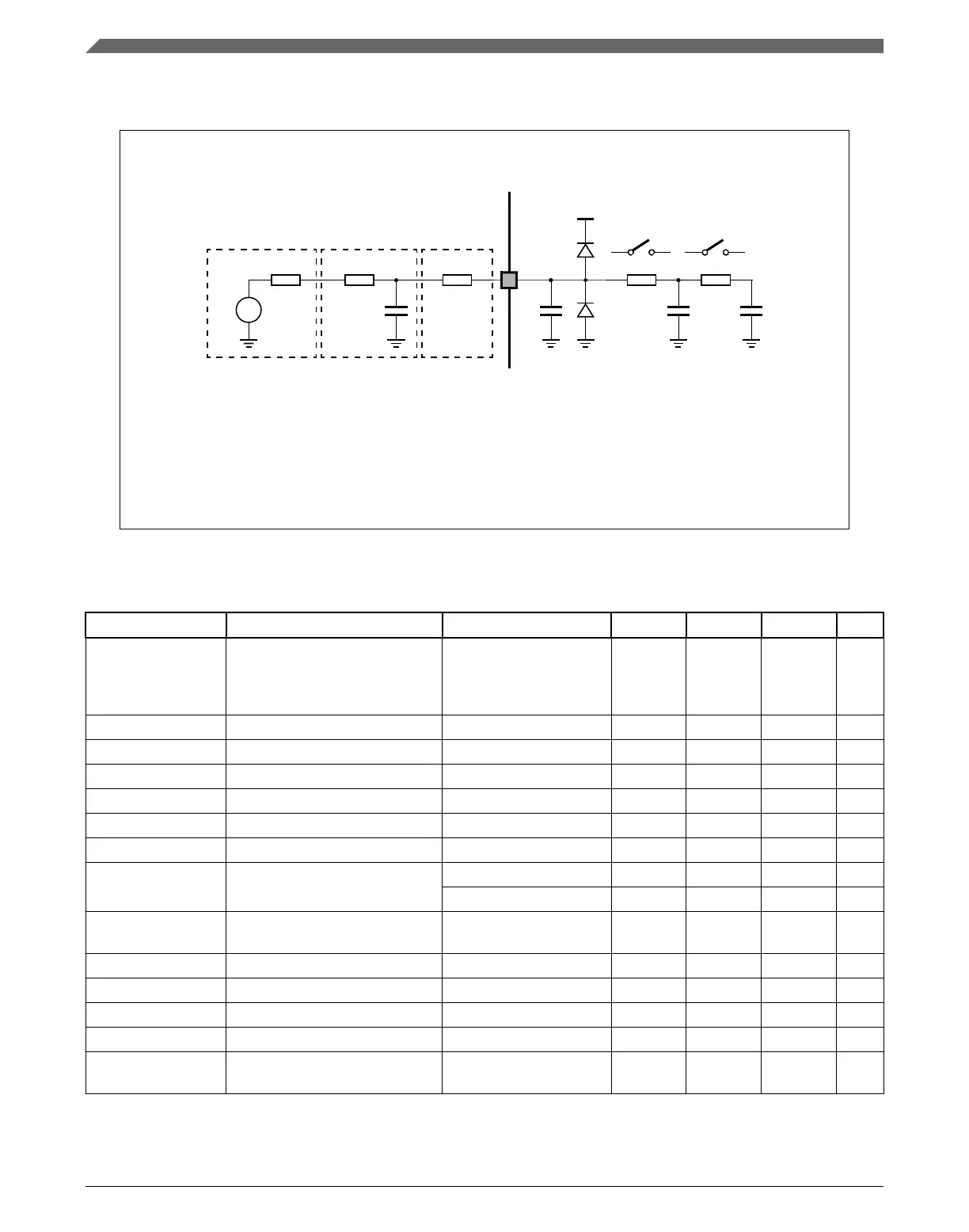
11.2.1 Input equivalent circuit and ADC conversion characteristics
R
F
C
F
R
S
R
L
R
SW1
C
P2
V
DD_HV_IO
Sampling
Source Filter Current Limiter
EXTERNAL CIRCUIT INTERNAL CIRCUIT SCHEME
R
S
Source Impedance
R
F
Filter Resistance
C
F
Filter Capacitance
R
L
Current Limiter Resistance
R
SW1
Channel Selection Switch Impedance
R
AD
Sampling Switch Impedance
C
P
Pin Capacitance (two contributions, C
P1
and C
P2
)
C
S
Sampling Capacitance
C
P1
R
AD
Channel
Selection
V
A
C
S
Figure 11. Input equivalent circuit
Table 19. ADC conversion characteristics
Symbol Parameter Conditions
1
Min Typ Max Unit
f
CK
, 2
ADC Clock frequency (depends
on ADC configuration) (The duty
cycle depends on AD_CK
3
frequency.)
— 20 — 80 MHz
f
s
Sampling frequency — — — 1.00 MHz
t
sample
Sample time
4
— 250 — — ns
t
conv
Conversion time
5
80 MHz 700 — — ns
C
S
, 6
ADC input sampling capacitance — — 3 5 pF
C
P1
6
ADC input pin capacitance 1 — — — 5 pF
C
P2
6
ADC input pin capacitance 2 — — — 0.8 pF
R
SW1
6
Internal resistance of analog
source
V
REF
range = 4.5 to 5.5 V — — 0.3 kΩ
V
REF
range = 3.0 to 3.6 V — — 875 Ω
R
AD
6
Internal resistance of analog
source
— — — 825 Ω
INL Integral non-linearity — –2 — 2 LSB
DNL Differential non-linearity — –1 — 1 LSB
OFS
7
Offset error — –6 — 6 LSB
GNE
7
Gain error — –6 — 6 LSB
Input (double ADC
channel)
Max leakage 150 °C — — 300 nA
Table continues on the next page...
ADC modules
SPC5746R Microcontroller Data Sheet, Rev. 6, 06/2017
28 NXP Semiconductors

 Loading...


