C
HV_PMC
C
HV_FLA
VSS
VDD_HV_FLA
VDD_HV_PMC
RAINIER
VDD_HV_IO
VSS
C
C
HV_ADC_D
VSS
VDD_LV
HV_IO
2
LV
1
VDD_HV_ADV_SD
VSS_HV_ADV_SD
1
One capacitance near each VDD_LV pin
2
One capacitance near each VDD_HV pin
HV_ADC_SAR
VDD_HV_ADV_SAR
VSS_HV_ADV_SAR
n x C
C
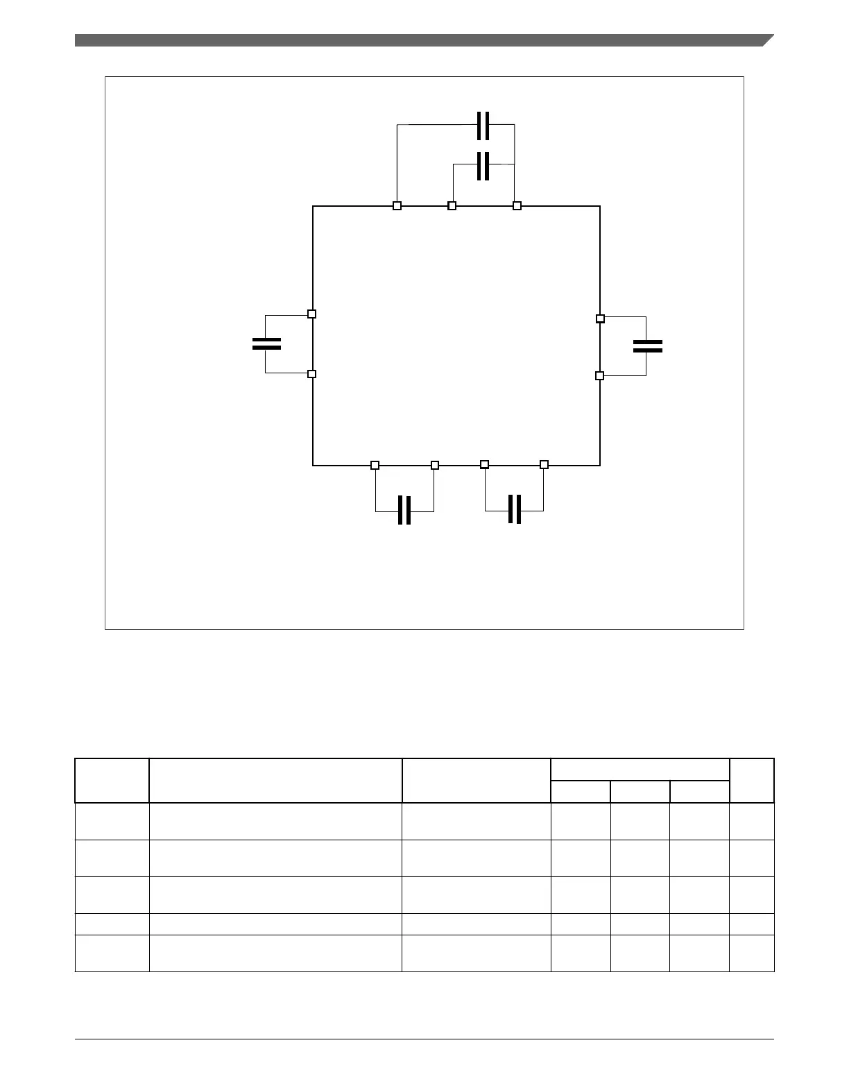
Figure 17. Recommended supply pin circuits
The following table describes the supply stability capacitances required on the device for
proper operation.
Table 28. Device power supply integration
Symbol Parameter Conditions
Value
1
Unit
Min Typ Max
C
LV
Minimum V
DD_LV
external bulk capacitance
,
2, 3
— 4.7 — — µF
C
HV_PMC
Minimum V
DD_HV_PMC
external bulk
capacitance
2, 4
— 4.7 — — µF
C
HV_IO
Minimum VDD_HV_IO external
capacitance
2
— 4.7 — — µF
C
HV_FLA
Minimum V
DD_HV_FLA
external capacitance
, 5
— 2.0 µF
C
HV_ADC_SA
R
Minimum V
DD_HV_ADV_SAR
external
capacitance
, 6
10 — — µF
Table continues on the next page...
Power management PMC POR LVD sequencing
SPC5746R Microcontroller Data Sheet, Rev. 6, 06/2017
NXP Semiconductors 49

 Loading...


