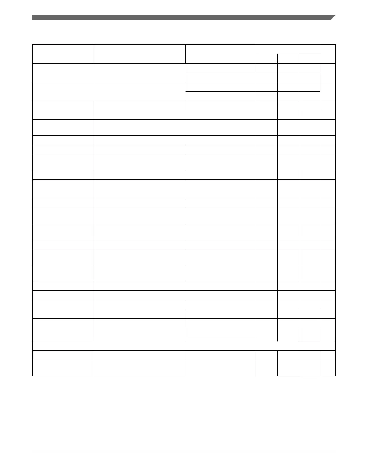
Table 3. Device operating conditions (continued)
Symbol Parameter Conditions
Value
Unit
Min Typ Max
V
DD_HV_IO_FEC
FEC I/O supply voltage
8
5 V range 3.5 — 5.5 V
3.3 V range 3.0 — 3.6
V
DD_HV_IO_MSC
MSC I/O supply voltage
9
5 V range 3.5 — 5.5 V
3.3 V range 3.0 — 3.6
V
DD_HV_IO_JTAG
10
JTAG I/O supply voltage
11
5 V range 3.5 — 5.5 V
3.3 V range 3.0 — 3.6
V
DD_HV_PMC
12
Power Management Controller
(PMC) supply voltage
Full functionality 3.5 — 5.5 V
V
DDSTBY
13
RAM standby supply voltage
14
— 1.3 — 5.9 V
V
STBY_BO
Standby RAM brownout voltage — — — 0.9 V
V
DD_LV_STBY_SW
Standby RAM switch V
DD_LV
voltage
threshold
—
0.95 — — V
V
DD_HV_ADV_SD
S/D ADC supply voltage
15, 16
— 4.5 — 5.5 V
V
DD_HV_ADV_SAR
SAR ADC supply voltage
17
—
3.0 — 5.5 V
V
DD_HV_ADR_SD
S/D ADC reference — 3.0 — 5.5 V
V
DD_HV_ADR_SD
–
V
DD_HV_ADV_SD
S/D ADC reference differential
voltage
—
— — 25 mV
V
SS_HV_ADR_SD
–
V
SS_HV_ADV_SD
V
SS_HV_ADR_SD
differential voltage
—
–25 — 25 mV
V
DD_HV_ADR_SAR
SAR ADC reference — 3.0 — 5.5 V
V
DD_HV_ADR_SAR
–
V
DD_HV_ADV_SAR
SAR ADC reference differential
voltage
—
— — 25 mV
V
SS_HV_ADR_SAR
–
V
SS_HV_ADV_SAR
V
SS_HV_ADR_SAR
differential voltage
—
–25 — 25 mV
V
SS_HV_ADV_SD
– V
SS
V
SS_HV_ADV_SD
differential voltage — –25 — 25 mV
V
SS_HV_ADV_SAR
– V
SS
V
SS_HV_ADV_SAR
differential voltage — –25 — 25 mV
V
RAMP_VDD_LV
Slew rate on power supply pins
(VDD_LV)
Ramp up 0.069 — 100 V/ms
Ramp down 0.0345 — 100
V
RAMP_VDD_HV_IO_MAIN
,
V
RAMP_VDD_HV_PMC
Slew rate on power supply pins
(VDD_HV_IO_MAIN,
VDD_HV_PMC)
Ramp up 0.148 — 100 V/ms
Ramp down 0.125 — 100
Injection current
I
IC
DC injection current (per pin)
18, 19, 20
Digital pins and analog pins –3.0 — 3.0 mA
I
MAXSEG
Maximum current per power
segment
21, 22
—
–80 — 80 mA
1. Maximum operating frequency is applicable to the computational cores and platform for the device.
2. Core voltage as measured on device pin to guarantee published silicon performance.
3. During power ramp, voltage measured on silicon might be lower. maximum performance is not guaranteed, but correct
silicon operation is guaranteed. See power management and reset management for description.
4. Maximum core voltage is not permitted for entire product life. See absolute maximum rating.
5. When internal LVD/HVDs are disabled, external monitoring is required to guarantee device operation. Failure to monitor
externally supply voltage may result in erroneous operation of the device.
Operating conditions
SPC5746R Microcontroller Data Sheet, Rev. 6, 06/2017
NXP Semiconductors 9

 Loading...


